ZHCS921A May 2012 – January 2016 ADS4128
PRODUCTION DATA.
- 1 特性
- 2 应用
- 3 说明
- 4 修订历史记录
- 5 Device Comparison Table
- 6 Pin Configuration and Functions
-
7 Specifications
- 7.1 Absolute Maximum Ratings
- 7.2 ESD Ratings
- 7.3 Recommended Operating Conditions
- 7.4 Thermal Information
- 7.5 Electrical Characteristics
- 7.6 Electrical Characteristics: General
- 7.7 Digital Characteristics
- 7.8 Timing Requirements: LVDS and CMOS Modes
- 7.9 Reset Timing Requirements
- 7.10 Typical Characteristics
- 7.11 Typical Characteristics: Contour
-
8 Detailed Description
- 8.1 Overview
- 8.2 Functional Block Diagram
- 8.3 Feature Description
- 8.4 Device Functional Modes
- 8.5 Programming
- 8.6 Register Maps
- 9 Application and Implementation
- 10Power Supply Recommendations
- 11Layout
- 12器件和文档支持
- 13机械、封装和可订购信息
6 Pin Configuration and Functions
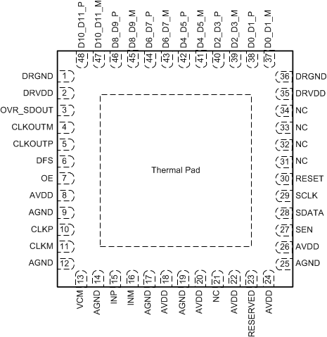
RGZ Package(1)
48-Pin VQFN With Exposed Thermal Pad
LVDS Mode - Top View

The thermal pad is connected to DRGND.
Pin Functions - LVDS Mode
| PIN | I/O | DESCRIPTION | |
|---|---|---|---|
| NAME | NO. | ||
| AGND | 9, 12, 14, 17, 19, 25 | I | Analog ground |
| AVDD | 8, 18, 20, 22, 24, 26 | I | 1.8-V analog power supply |
| CLKM | 11 | I | Differential clock input, negative |
| CLKP | 10 | I | Differential clock input, positive |
| CLKOUTM | 4 | O | Differential output clock, negative |
| CLKOUTP | 5 | O | Differential output clock, positive |
| D0_D1_P | 38 | O | Differential output data D0 and D1 multiplexed, true |
| D0_D1_M | 37 | O | Differential output data D0 and D1 multiplexed, complement |
| D2_D3_P | 40 | O | Differential output data D2 and D3 multiplexed, true |
| D2_D3_M | 39 | O | Differential output data D2 and D3 multiplexed, complement |
| D4_D5_P | 42 | O | Differential output data D4 and D5 multiplexed, true |
| D4_D5_M | 41 | O | Differential output data D4 and D5 multiplexed, complement |
| D6_D7_P | 44 | O | Differential output data D6 and D7 multiplexed, true |
| D6_D7_M | 43 | O | Differential output data D6 and D7 multiplexed, complement |
| D8_D9_P | 46 | O | Differential output data D8 and D9 multiplexed, true |
| D8_D9_M | 45 | O | Differential output data D8 and D9 multiplexed, complement |
| D10_D11_P | 48 | O | Differential output data D10 and D11 multiplexed, true |
| D10_D11_M | 47 | O | Differential output data D10 and D11 multiplexed, complement |
| DFS | 6 | I | Data format select input. This pin sets the DATA FORMAT (twos complement or offset binary) and the LVDS and CMOS output interface type. See Table 9 for detailed information. |
| DRGND | 1, 36, PAD | I | Digital and output buffer ground |
| DRVDD | 2, 35 | I | 1.8-V digital and output buffer supply |
| INM | 16 | I | Differential analog input, negative |
| INP | 15 | I | Differential analog input, positive |
| NC | 21, 31, 32, 33, 34 | — | Do not connect |
| OE | 7 | I | Output buffer enable input, active high; this pin has an internal 180-kΩ pull-up resistor to DRVDD. |
| OVR_SDOUT | 3 | O | This pin functions as an out-of-range indicator after reset when register bit READOUT = 0, and functions as a serial register readout pin when READOUT = 1. |
| RESERVED | 23 | I | Digital control pin, reserved for future use |
| RESET | 30 | I | Serial interface RESET input. When using the serial interface mode, the internal registers must initialize through hardware RESET by applying a high pulse on this pin or by using the software reset option; refer to the Serial Interface section. When RESET is tied high, the internal registers are reset to the default values. In this condition, SEN can be used as an analog control pin. RESET has an internal 180-kΩ pull-down resistor. |
| SCLK | 29 | I | This pin functions as a serial interface clock input when RESET is low. When RESET is high, SCLK has no function and should be tied to ground. This pin has an internal 180-kΩ pull-down resistor. |
| SDATA | 28 | I | This pin functions as a serial interface data input when RESET is low. When RESET is high, SDATA functions as a STANDBY control pin (see Table 11). This pin has an internal 180-kΩ pull-down resistor. |
| SEN | 27 | I | This pin functions as a serial interface enable input when RESET is low. When RESET is high, SEN has no function and should be tied to AVDD. This pin has an internal 180-kΩ pull-up resistor to AVDD. |
| VCM | 13 | O | Outputs the common-mode voltage (0.95 V) that can be used externally to bias the analog input pins. |
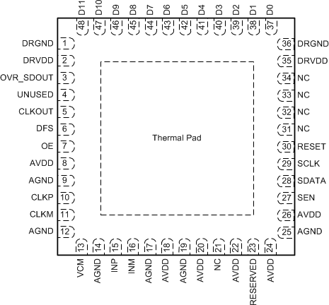
RGZ Package(2)
48-Pin VQFN With Exposed Thermal Pad
CMOS - Top View

The thermal pad is connected to DRGND.
Pin Functions - CMOS Mode
| PIN | I/O | DESCRIPTION | |
|---|---|---|---|
| NAME | NO. | ||
| AGND | 9, 12, 14, 17, 19, 25 | I | Analog ground |
| AVDD | 8, 18, 20, 22, 24, 26 | I | 1.8-V analog power supply |
| CLKM | 11 | I | Differential clock input, negative |
| CLKP | 10 | I | Differential clock input, positive |
| CLKOUT | 5 | O | CMOS output clock |
| D0 | 37 | O | 12-bit CMOS output data |
| D1 | 38 | O | 12-bit CMOS output data |
| D2 | 39 | O | 12-bit CMOS output data |
| D3 | 40 | O | 12-bit CMOS output data |
| D4 | 41 | O | 12-bit CMOS output data |
| D5 | 42 | O | 12-bit CMOS output data |
| D6 | 43 | O | 12-bit CMOS output data |
| D7 | 44 | O | 12-bit CMOS output data |
| D8 | 45 | O | 12-bit CMOS output data |
| D9 | 46 | O | 12-bit CMOS output data |
| D10 | 47 | O | 12-bit CMOS output data |
| D11 | 48 | O | 12-bit CMOS output data |
| DFS | 6 | I | Data format select input. This pin sets the DATA FORMAT (twos complement or offset binary) and the LVDS and CMOS output interface type. See Table 9 for detailed information. |
| DRGND | 1, 36, PAD | I | Digital and output buffer ground |
| DRVDD | 2, 35 | I | 1.8-V digital and output buffer supply |
| INP | 15 | I | Differential analog input, positive |
| INM | 16 | I | Differential analog input, negative |
| NC | 21, 31, 32, 33, 34 | — | Do not connect |
| OE | 7 | I | Output buffer enable input, active high; this pin has an internal 180-kΩ pull-up resistor to DRVDD. |
| OVR_SDOUT | 3 | O | This pin functions as an out-of-range indicator after reset when register bit READOUT = 0, and functions as a serial register readout pin when READOUT = 1. |
| RESET | 30 | I | Serial interface RESET input. When using the serial interface mode, the internal registers must initialize through hardware RESET by applying a high pulse on this pin or by using the software reset option; refer to the Serial Interface section. When RESET is tied high, the internal registers are reset to the default values. In this condition, SEN can be used as an analog control pin. RESET has an internal 180-kΩ pull-down resistor. |
| RESERVED | 23 | I | Digital control pin, reserved for future use |
| SCLK | 29 | I | This pin functions as a serial interface clock input when RESET is low. When RESET is high, SCLK has no function and should be tied to ground. This pin has an internal 180-kΩ pull-down resistor. |
| SDATA | 28 | I | This pin functions as a serial interface data input when RESET is low. When RESET is high, SDATA functions as a STANDBY control pin (see Table 11). This pin has an internal 180-kΩ pull-down resistor. |
| SEN | 27 | I | This pin functions as a serial interface enable input when RESET is low. When RESET is high, SEN has no function and should be tied to AVDD. This pin has an internal 180-kΩ pull-up resistor to AVDD. |
| UNUSED | 4 | — | Unused pin in CMOS mode |
| VCM | 13 | O | Outputs the common-mode voltage (0.95 V) that can be used externally to bias the analog input pins. |