ZHCS921A May 2012 – January 2016 ADS4128
PRODUCTION DATA.
- 1 特性
- 2 应用
- 3 说明
- 4 修订历史记录
- 5 Device Comparison Table
- 6 Pin Configuration and Functions
-
7 Specifications
- 7.1 Absolute Maximum Ratings
- 7.2 ESD Ratings
- 7.3 Recommended Operating Conditions
- 7.4 Thermal Information
- 7.5 Electrical Characteristics
- 7.6 Electrical Characteristics: General
- 7.7 Digital Characteristics
- 7.8 Timing Requirements: LVDS and CMOS Modes
- 7.9 Reset Timing Requirements
- 7.10 Typical Characteristics
- 7.11 Typical Characteristics: Contour
-
8 Detailed Description
- 8.1 Overview
- 8.2 Functional Block Diagram
- 8.3 Feature Description
- 8.4 Device Functional Modes
- 8.5 Programming
- 8.6 Register Maps
- 9 Application and Implementation
- 10Power Supply Recommendations
- 11Layout
- 12器件和文档支持
- 13机械、封装和可订购信息
7 Specifications
7.1 Absolute Maximum Ratings
over operating free-air temperature range (unless otherwise noted)(1)| MIN | MAX | UNIT | ||
|---|---|---|---|---|
| Supply voltage | AVDD | –0.3 | 2.1 | V |
| DRVDD | –0.3 | 2.1 | ||
| Voltage | Between AGND and DRGND | –0.3 | 0.3 | V |
| Between AVDD to DRVDD (when AVDD leads DRVDD) | 0 | 2.1 | ||
| Between DRVDD to AVDD (when DRVDD leads AVDD) | 0 | 2.1 | ||
| Voltage applied to input pins | INP, INM | –0.3 | (1.9) AVDD + 0.3 | V |
| CLKP, CLKM(2), DFS, OE | –0.3 | AVDD + 0.3 | ||
| RESET, SCLK, SDATA, SEN | –0.3 | 3.9 | ||
| Temperature | Operating free-air, TA | –40 | 85 | °C |
| Operating junction, TJ | 125 | |||
| Storage, Tstg | –65 | 150 | °C | |
(1) Stresses beyond those listed under Absolute Maximum Ratings may cause permanent damage to the device. These are stress ratings only, which do not imply functional operation of the device at these or any other conditions beyond those indicated under Recommended Operating Conditions. Exposure to absolute-maximum-rated conditions for extended periods may affect device reliability.
(2) When AVDD is turned off, it is recommended to switch off the input clock (or ensure the voltage on CLKP and CLKM is less than |0.3 V|. This setting prevents the ESD protection diodes at the clock input pins from turning on.
7.2 ESD Ratings
| VALUE | UNIT | |||
|---|---|---|---|---|
| V(ESD) | Electrostatic discharge | Human-body model (HBM), per ANSI/ESDA/JEDEC JS-001(1) | ±1000 | V |
| Charged-device model (CDM), per JEDEC specification JESD22-C101(2) | ±500 | |||
(1) JEDEC document JEP155 states that 500-V HBM allows safe manufacturing with a standard ESD control process.
(2) JEDEC document JEP157 states that 250-V CDM allows safe manufacturing with a standard ESD control process.
7.3 Recommended Operating Conditions
Over operating free-air temperature range, unless otherwise noted.| MIN | TYP | MAX | UNIT | ||
|---|---|---|---|---|---|
| SUPPLIES | |||||
| AVDD | Analog supply voltage | 1.7 | 1.8 | 1.9 | V |
| DRVDD | Digital supply voltage | 1.7 | 1.8 | 1.9 | |
| ANALOG INPUTS | |||||
| Differential input voltage range(1) | 2 | VPP | |||
| Input common-mode voltage | VCM ± 0.05 | V | |||
| Maximum analog input frequency | With 2-VPP input amplitude(2) | 400 | MHz | ||
| With 1-VPP input amplitude(2) | 800 | ||||
| CLOCK INPUT | |||||
| Input clock sample rate, low-speed mode | Enabled(3) | 20 | 80 | MSPS | |
| Disabled(3) | > 80 | 200 | |||
| Input clock amplitude differential (VCLKP – VCLKM) | Sine wave, ac-coupled | 0.2 | 1.5 | VPP | |
| LVPECL, ac-coupled | 1.6 | ||||
| LVDS, ac-coupled | 0.7 | ||||
| LVCMOS, single-ended, ac-coupled | 1.8 | V | |||
| Input clock duty cycle | Low-speed mode enabled | 40% | 50% | 60% | |
| Low-speed mode disabled | 35% | 50% | 65% | ||
| DIGITAL OUTPUTS | |||||
| CLOAD | Maximum external load capacitance from each output pin to DRGND | 5 | pF | ||
| RLOAD | Differential load resistance between the LVDS output pairs (LVDS mode) | 100 | Ω | ||
| TA | Operating free-air temperature | –40 | 85 | °C | |
(1) With 0-dB gain. See the Fine Gain section in the Detailed Description for relation between input voltage range and gain.
(2) See the Overview section in the Detailed Description.
(3) It is recommended to use these modes to get best performance. These modes can be set using the serial interface only.
7.4 Thermal Information
| THERMAL METRIC(1) | ADS4128 | UNIT | |
|---|---|---|---|
| RGZ (VQFN) | |||
| 48 PINS | |||
| RθJA | Junction-to-ambient thermal resistance | 27.9 | °C/W |
| RθJC(top) | Junction-to-case (top) thermal resistance | 15.1 | °C/W |
| RθJB | Junction-to-board thermal resistance | 5.4 | °C/W |
| ψJT | Junction-to-top characterization parameter | 0.3 | °C/W |
| ψJB | Junction-to-board characterization parameter | 5.4 | °C/W |
| RθJC(bot) | Junction-to-case (bottom) thermal resistance | 1.7 | °C/W |
(1) For more information about traditional and new thermal metrics, see the Semiconductor and IC Package Thermal Metrics application report, SPRA953.
7.5 Electrical Characteristics
Typical values are at 25°C, AVDD = 1.8 V, DRVDD = 1.8 V, 50% clock duty cycle, –1-dBFS differential analog input, 1-dB gain, and DDR LVDS interface, unless otherwise noted.Minimum and maximum values are across the full temperature range: TMIN = –40°C to TMAX = 85°C, AVDD = 1.8 V, and DRVDD = 1.8 V. Note that after reset, the device is in 0-dB gain mode.
| PARAMETER | TEST CONDITIONS | MIN | TYP | MAX | UNIT | |
|---|---|---|---|---|---|---|
| Resolution | 12 | Bits | ||||
| SNR | Signal-to-noise ratio, LVDS | fIN = 10 MHz | 70 | dBFS | ||
| fIN = 70 MHz | 70 | |||||
| fIN = 100 MHz | 69.7 | |||||
| fIN = 170 MHz | 65.8 | 69 | ||||
| fIN = 300 MHz | 68.2 | |||||
| SINAD | Signal-to-noise and distortion ratio, LVDS | fIN = 10 MHz | 69.8 | dBFS | ||
| fIN = 70 MHz | 69.2 | |||||
| fIN = 100 MHz | 69.1 | |||||
| fIN = 170 MHz | 65.5 | 68.8 | ||||
| fIN = 300 MHz | 67 | |||||
| SFDR | Spurious-free dynamic range | fIN = 10 MHz | 87 | dBc | ||
| fIN = 70 MHz | 80 | |||||
| fIN = 100 MHz | 82 | |||||
| fIN = 170 MHz | 70 | 85 | ||||
| fIN = 300 MHz | 74 | |||||
| THD | Total harmonic distortion | fIN = 10 MHz | 84 | dBc | ||
| fIN = 70 MHz | 78 | |||||
| fIN = 100 MHz | 79 | |||||
| fIN = 170 MHz | 69 | 83 | ||||
| fIN = 300 MHz | 73 | |||||
| HD2 | Second-harmonic distortion | fIN = 10 MHz | 90 | dBc | ||
| fIN = 70 MHz | 84 | |||||
| fIN = 100 MHz | 83 | |||||
| fIN = 170 MHz | 70 | 85 | ||||
| fIN = 300 MHz | 74 | |||||
| HD3 | Third-harmonic distortion | fIN = 10 MHz | 87 | dBc | ||
| fIN = 70 MHz | 80 | |||||
| fIN = 100 MHz | 82 | |||||
| fIN = 170 MHz | 70 | 86 | ||||
| fIN = 300 MHz | 79 | |||||
| Worst spur (other than second and third harmonics) |
fIN = 10 MHz | 93 | dBc | |||
| fIN = 70 MHz | 93 | |||||
| fIN = 100 MHz | 91 | |||||
| fIN = 170 MHz | 75 | 90 | ||||
| fIN = 300 MHz | 88 | |||||
| IMD | Two-tone intermodulation distortion | f1 = 46 MHz, f2 = 50 MHz, each tone at –7 dBFS |
–85 | dBFS | ||
| f1 = 185 MHz, f2 = 190 MHz, each tone at –7 dBFS |
–90 | |||||
| Input overload recovery | Recovery to within 1% (of final value) for 6-dB overload with sine-wave input | 1 | Clock cycles | |||
| PSRR | AC power-supply rejection ratio | For 50-mVPP signal on AVDD supply, up to 10 MHz |
> 30 | dB | ||
| ENOB | Effective number of bits | fIN = 170 MHz | 11.2 | LSBs | ||
| DNL | Differential nonlinearity | fIN = 170 MHz | –0.95 | ±0.2 | 1.6 | LSBs |
| INL | Integrated nonlinearity | fIN = 170 MHz | ±0.5 | ±5 | LSBs | |
7.6 Electrical Characteristics: General
Typical values are at 25°C, AVDD = 1.8 V, DRVDD = 1.8 V, 50% clock duty cycle, and 0-dB gain, unless otherwise noted.Minimum and maximum values are across the full temperature range: TMIN = –40°C to TMAX = 85°C, AVDD = 1.8 V, and DRVDD = 1.8 V.
| PARAMETER | TEST CONDITIONS | MIN | TYP | MAX | UNIT | |
|---|---|---|---|---|---|---|
| ANALOG INPUTS | ||||||
| Differential input voltage range | 2 | VPP | ||||
| Differential input resistance (at dc); see Figure 47 | > 1 | MΩ | ||||
| Differential input capacitance; see Figure 48 | 4 | pF | ||||
| Analog input bandwidth | 550 | MHz | ||||
| Analog input common-mode current (per input pin) | 0.6 | µA/MSPS | ||||
| VCM | Common-mode output voltage | 0.95 | V | |||
| VCM output current capability | 4 | mA | ||||
| DC ACCURACY | ||||||
| Offset error | –15 | 2.5 | 15 | mV | ||
| Temperature coefficient of offset error | 0.003 | mV/°C | ||||
| EGREF | Gain error as a result of internal reference inaccuracy alone | –2 | 2 | %FS | ||
| EGCHAN | Gain error of channel alone | –0.2 | ±1 | %FS | ||
| Temperature coefficient of EGCHAN | 0.001 | Δ%/°C | ||||
| POWER SUPPLY | ||||||
| IAVDD | Analog supply current | 85 | 113 | mA | ||
| IDRVDD(2) | Output buffer supply current, LVDS interface with 100-Ω external termination | Low LVDS swing (200 mV) | 43 | mA | ||
| Standard LVDS swing (350 mV) | 55 | 72 | ||||
| Output buffer supply current(2)(1)
CMOS interface |
8-pF external load capacitance fIN = 2.5 MHz |
33 | ||||
| Analog power | 153 | mW | ||||
| Digital power, LVDS interface | Low LVDS swing (200 mV) | 77 | mW | |||
| Digital power, CMOS interface(1) | 8-pF external load capacitance fIN = 2.5 MHz |
59 | mW | |||
| Global power-down | 10 | 25 | mW | |||
| Standby | 185 | mW | ||||
(1) In CMOS mode, the DRVDD current scales with the sampling frequency, the load capacitance on the output pins, input frequency, and the supply voltage (see the CMOS Interface Power Dissipation section in the Device Functional Modes).
(2) The maximum DRVDD current with CMOS interface depends on the actual load capacitance on the digital output lines. Note that the maximum recommended load capacitance on each digital output line is 10 pF.
7.7 Digital Characteristics
Typical values are at 25°C, AVDD = 1.8 V, DRVDD = 1.8 V, and 50% clock duty cycle, unless otherwise noted.Minimum and maximum values are across the full temperature range: TMIN = –40°C to TMAX = 85°C, AVDD = 1.8 V, and DRVDD = 1.8 V.
| PARAMETER | TEST CONDITIONS | MIN | TYP | MAX | UNIT | |
|---|---|---|---|---|---|---|
| DIGITAL INPUTS (RESET, SCLK, SDATA, SEN, OE) | ||||||
| VIH | High-level input voltage | RESET, SCLK, SDATA, and SEN support 1.8-V and 3.3-V CMOS logic levels | 1.3 | V | ||
| OE only supports 1.8-V CMOS logic levels | 1.3 | |||||
| VIL | Low-level input voltage | RESET, SCLK, SDATA, and SEN support 1.8-V and 3.3-V CMOS logic levels | 0.4 | V | ||
| OE only supports 1.8-V CMOS logic levels | 0.4 | |||||
| IIH | High-level input current, SDATA and SCLK(1) | VHIGH = 1.8 V | 10 | µA | ||
| High-level input current, SEN | VHIGH = 1.8 V | 0 | ||||
| IIL | Low-level input, SDATA and SCLK | VLOW = 0 V | 0 | µA | ||
| Low-level input, SEN | VLOW = 0 V | 10 | ||||
| DIGITAL OUTPUTS (CMOS INTERFACE: D0 to D11, OVR_SDOUT) | ||||||
| VOH | High-level output voltage | DRVDD – 0.1 | DRVDD | V | ||
| VOL | Low-level output voltage | 0 | 0.1 | V | ||
| DIGITAL OUTPUTS (LVDS INTERFACE: DA0P and DA0M to DA11P and DA11M, DB0P and DB0M to DB11P and DB11M, CLKOUTP and CLKOUTM) | ||||||
| VODH | High-level output voltage(2) | Standard-swing LVDS | 270 | 350 | 430 | mV |
| Low-swing LVDS | 200 | |||||
| VODL | Low-level output voltage(2) | Standard-swing LVDS | –430 | –350 | –270 | mV |
| Low-swing LVDS | –200 | |||||
| VOCM | Output common-mode voltage | 0.85 | 1.05 | 1.25 | V | |
(1) SDATA and SCLK have an internal 180-kΩ pull-down resistor.
(2) With an external 100-Ω termination.
7.8 Timing Requirements: LVDS and CMOS Modes(1)
Typical values are at 25°C, AVDD = 1.8 V, DRVDD = 1.8 V, sampling frequency = 200 MSPS, sine wave input clock,CLOAD = 5 pF(2), and RLOAD = 100 Ω(3), unless otherwise noted. Minimum and maximum values are across the full temperature range: TMIN = –40°C to TMAX = 85°C, AVDD = 1.8 V, and DRVDD = 1.7 V to 1.9 V.
| MIN | NOM | MAX | UNIT | |||
|---|---|---|---|---|---|---|
| tA | Aperture delay | 0.6 | 0.8 | 1.2 | ns | |
| Aperture delay variation | Between two devices at the same temperature and DRVDD supply | ±100 | ps | |||
| tJ | Aperture jitter | 100 | fS rms | |||
| Wakeup time | Time to valid data after coming out of STANDBY mode | 5 | 25 | µs | ||
| Time to valid data after coming out of PDN GLOBAL mode | 100 | 500 | ||||
| ADC latency(8) | Low-latency mode (default after reset) | 10 | Clock cycles | |||
| Low-latency mode disabled (gain enabled, offset correction disabled) |
16 | |||||
| Low-latency mode disabled (gain and offset correction enabled) |
17 | |||||
| DDR LVDS MODE(4)(5) | ||||||
| tSU | Data setup time(3) | Data valid(6) to zero-crossing of CLKOUTP | 1.05 | 1.55 | ns | |
| tH | Data hold time(3) | Zero-crossing of CLKOUTP to data becoming invalid(6) | 0.35 | 0.6 | ns | |
| tPDI | Clock propagation delay | Input clock rising edge crossover to output clock rising edge crossover 1 MSPS ≤ sampling frequency ≤ 200 MSPS |
3 | 4.2 | 5.4 | ns |
| Variation of tPDI | Between two devices at the same temperature and DRVDD supply | ±0.6 | ns | |||
| LVDS bit clock duty cycle | Duty cycle of differential clock, (CLKOUTP – CLKOUTM) 1 MSPS ≤ sampling frequency ≤ 200 MSPS |
42% | 48% | 54% | ||
| tRISE, tFALL | Data rising time, Data falling time |
Rising time measured from –100 mV to 100 mV Falling time measured from 100 mV to –100 mV 1 MSPS ≤ sampling frequency ≤ 200 MSPS |
0.14 | ns | ||
| tCLKRISE, tCLKFALL |
Output clock rising time, Output clock falling time |
Rising time measured from –100 mV to 100 mV Falling time measured from 100 mV to –100 mV 1 MSPS ≤ sampling frequency ≤ 200 MSPS |
0.14 | ns | ||
| tOE | Output enable (OE) to data delay | Time to valid data after OE becomes active | 50 | 100 | ns | |
| PARALLEL CMOS MODE(7) | ||||||
| tSTART | Input clock to data delay | Input clock rising edge crossover to start of data valid(6) | –0.3 | ns | ||
| tDV | Data valid time | Time interval of valid data(6) | 3.5 | 4.2 | ns | |
| tPDI | Clock propagation delay | Input clock rising edge crossover to output clock rising edge crossover 1 MSPS ≤ sampling frequency ≤ 200 MSPS |
4 | 5.5 | 7 | ns |
| Output clock duty cycle | Duty cycle of output clock, CLKOUT 1 MSPS ≤ sampling frequency ≤ 200 MSPS |
47% | ||||
| tRISE, tFALL | Data rising time, Data falling time |
Rising time measured from 20% to 80% of DRVDD Falling time measured from 80% to 20% of DRVDD 1 ≤ sampling frequency ≤ 200 MSPS |
0.35 | ns | ||
| tCLKRISE, tCLKFALL |
Output clock rising time, Output clock falling time |
Rising time measured from 20% to 80% of DRVDD Falling time measured from 80% to 20% of DRVDD 1 ≤ sampling frequency ≤ 200 MSPS |
0.35 | ns | ||
| tOE | Output enable (OE) to data delay | Time to valid data after OE becomes active | 20 | 40 | ns | |
(1) Timing parameters are ensured by design and characterization but are not production tested.
(2) CLOAD is the effective external single-ended load capacitance between each output pin and ground.
(3) RLOAD is the differential load resistance between the LVDS output pair.
(4) Measurements are done with a transmission line of 100-Ω characteristic impedance between the device and the load. Setup and hold time specifications take into account the effect of jitter on the output data and clock.
(5) The LVDS timings are unchanged for low latency disabled and enabled.
(6) Data valid refers to a logic high of 1.26 V and a logic low of 0.54 V.
(7) Low-latency mode enabled.
(8) At higher frequencies, tPDI is greater than one clock period and overall latency = ADC latency + 1.
7.9 Reset Timing Requirements
Typical values are at 25°C and minimum and maximum values are across the full temperature range: TMIN = –40°C to TMAX = 85°C, unless otherwise noted.| MIN | TYP | MAX | UNIT | |||
|---|---|---|---|---|---|---|
| t1 | Power-on delay | Delay from power-up of AVDD and DRVDD to RESET pulse active | 1 | ms | ||
| t2 | Reset pulse width | Pulse width of active RESET signal that resets the serial registers | 10 | ns | ||
| 1(1) | µs | |||||
| t3 | Delay from RESET disable to SEN active | 100 | ns | |||
(1) The reset pulse is needed only when using the serial interface configuration. If the pulse width is greater than 1 µs, the device can enter the parallel configuration mode briefly and then return back to serial interface mode.
Table 1. LVDS Timing Across Sampling Frequencies
| SAMPLING FREQUENCY (MSPS) | SETUP TIME (ns) | HOLD TIME (ns) | ||||
|---|---|---|---|---|---|---|
| MIN | TYP | MAX | MIN | TYP | MAX | |
| 200 | 1.05 | 1.55 | — | 0.35 | 0.6 | — |
| 185 | 1.1 | 1.7 | — | 0.35 | 0.6 | — |
| 160 | 1.6 | 2.1 | — | 0.35 | 0.6 | — |
| 125 | 2.3 | 3 | — | 0.35 | 0.6 | — |
| 80 | 4.5 | 5.2 | — | 0.35 | 0.6 | — |
Table 2. CMOS Timing Across Sampling Frequencies (Low Latency Enabled)
| SAMPLING FREQUENCY (MSPS) | TIMING SPECIFIED WITH RESPECT TO OUTPUT CLOCK | ||||||||
|---|---|---|---|---|---|---|---|---|---|
| tSETUP (ns) | tHOLD (ns) | tPDI (ns) | |||||||
| MIN | TYP | MAX | MIN | TYP | MAX | MIN | TYP | MAX | |
| 200 | 1.6 | 2.2 | — | 1.8 | 2.5 | — | 4 | 5.5 | 7 |
| 185 | 1.8 | 2.4 | — | 1.9 | 2.7 | — | 4 | 5.5 | 7 |
| 160 | 2.3 | 2.9 | — | 2.2 | 3 | — | 4 | 5.5 | 7 |
| 125 | 3.1 | 3.7 | — | 3.2 | 4 | — | 4 | 5.5 | 7 |
| 80 | 5.4 | 6 | — | 5.4 | 6 | — | 4 | 5.5 | 7 |
Table 3. CMOS Timing Across Sampling Frequencies (Low Latency Disabled)
| SAMPLING FREQUENCY (MSPS) | TIMING SPECIFIED WITH RESPECT TO OUTPUT CLOCK | ||||||||
|---|---|---|---|---|---|---|---|---|---|
| tSETUP (ns) | tHOLD (ns) | tPDI (ns) | |||||||
| MIN | TYP | MAX | MIN | TYP | MAX | MIN | TYP | MAX | |
| 200 | 1 | 1.6 | — | 2 | 2.8 | — | 4 | 5.5 | 7 |
| 185 | 1.3 | 2 | — | 2.2 | 3 | — | 4 | 5.5 | 7 |
| 160 | 1.8 | 2.5 | — | 2.5 | 3.3 | — | 4 | 5.5 | 7 |
| 125 | 2.5 | 3.2 | — | 3.5 | 4.3 | — | 4 | 5.5 | 7 |
| 80 | 4.8 | 5.5 | — | 5.7 | 6.5 | — | 4 | 5.5 | 7 |
Table 4. CMOS Timing Across Sampling Frequencies (Low Latency Enabled)
| SAMPLING FREQUENCY (MSPS) | TIMING SPECIFIED WITH RESPECT TO INPUT CLOCK | |||||
|---|---|---|---|---|---|---|
| tSTART (ns) | tDV (ns) | |||||
| MIN | TYP | MAX | MIN | TYP | MAX | |
| 200 | — | — | –0.3 | 3.5 | 4.2 | — |
| 185 | — | — | –1 | 3.9 | 4.5 | — |
| 170 | — | — | –1.5 | 4.3 | 5 | — |
Table 5. CMOS Timing Across Sampling Frequencies (Low Latency Disabled)
| SAMPLING FREQUENCY (MSPS) | TIMING SPECIFIED WITH RESPECT TO INPUT CLOCK | |||||
|---|---|---|---|---|---|---|
| tSTART (ns) | tDV (ns) | |||||
| MIN | TYP | MAX | MIN | TYP | MAX | |
| 200 | — | — | 0.3 | 3.5 | 4.2 | — |
| 185 | — | — | 0 | 3.9 | 4.5 | — |
| 170 | — | — | –1.3 | 4.3 | 5 | — |
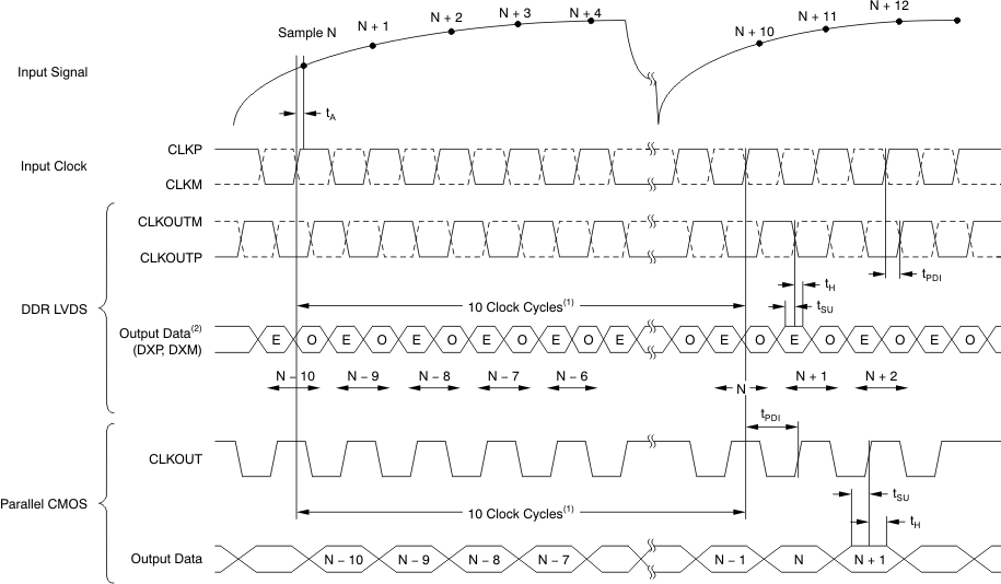
ADC latency in low-latency mode. At higher sampling frequencies, tDPI is greater than one clock cycle which then makes the overall latency = ADC latency + 1.
E = Even bits (D0, D2, D4, and so on). O = Odd bits (D1, D3, D5, and so on).
Figure 1. Latency Diagram
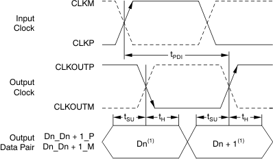
Dn = bits D0, D2, D4, and so on. Dn + 1 = bits D1, D3, D5, and so on.
Figure 2. LVDS Mode Timing
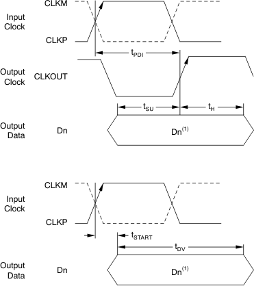
Dn = bits D0, D1, D2, and so forth.
Figure 3. CMOS Mode Timing

With external 100-Ω termination.
Figure 4. LVDS Output Voltage Levels
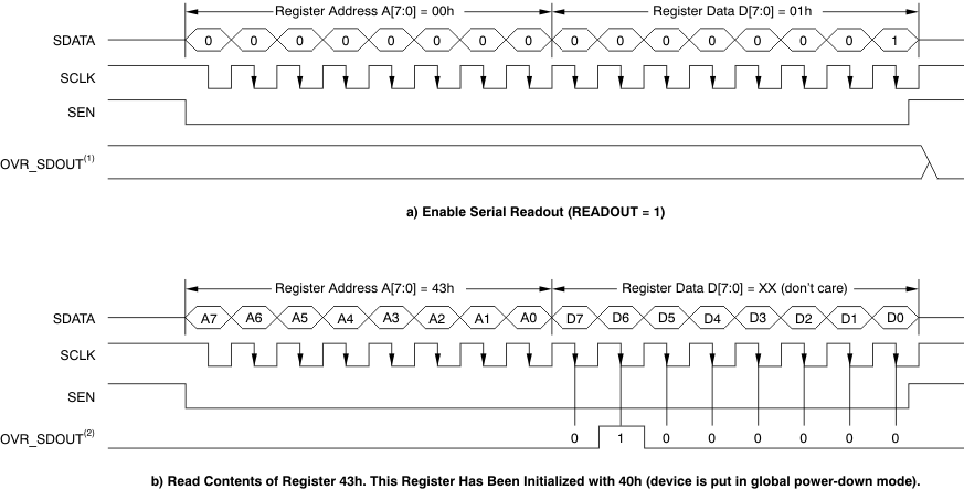
The OVR_SDOUT pin functions as OVR (READOUT = 0).
The OVR_SDOUT pin functions as a serial readout (READOUT = 1).
Figure 5. Serial Readout Timing Diagram
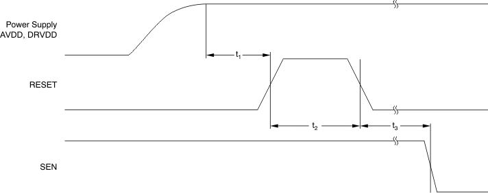
A high pulse on the RESET pin is required in the serial interface mode in case of initialization through hardware reset. For parallel interface operation, RESET must be permanently tied high.
Figure 6. Reset Timing Diagram
 Figure 7. Serial Interface Timing
7.10 Typical Characteristics
At 25°C, AVDD = 1.8 V, DRVDD = 1.8 V, maximum rated sampling frequency, sine wave input clock, 1.5-VPP differential clock amplitude, 50% clock duty cycle, –1-dBFS differential analog input, 0-dB gain, low-latency mode, DDR LVDS output interface, and 32k-point FFT, unless otherwise noted.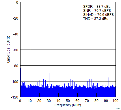 Figure 8. FFT for 10-MHz Input Signal
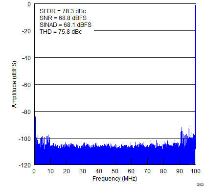 Figure 10. FFT for 300-MHz Input Signal
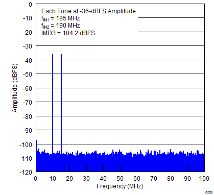 Figure 12. FFT for Two-Tone Input Signal
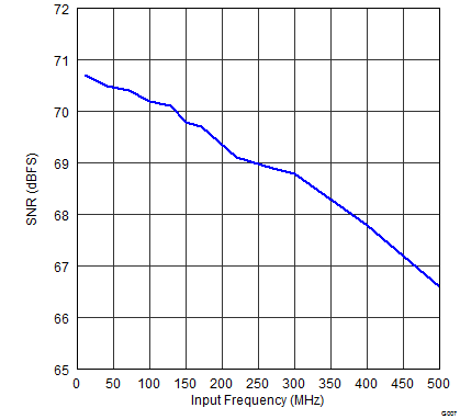 Figure 14. SNR vs Input Frequency
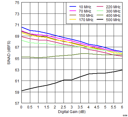 Figure 16. SINAD vs Digital Gain
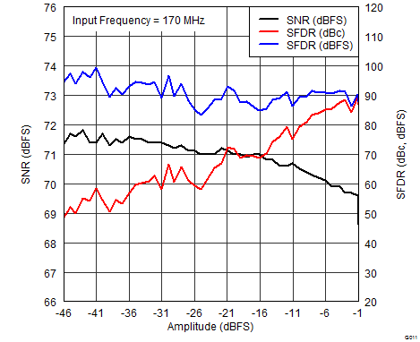 Figure 18. Performance Across Input Amplitude
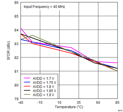 Figure 20. SFDR vs AVDD Supply and Temperature
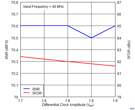 Figure 22. Performance vs DRVDD Supply
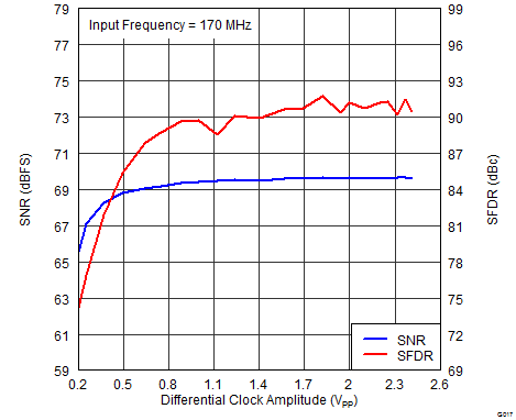 Figure 24. Performance vs Clock Amplitude
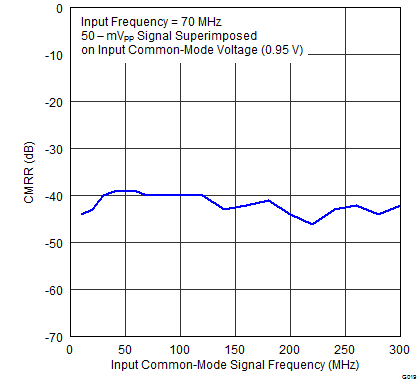 Figure 26. CMRR vs Frequency
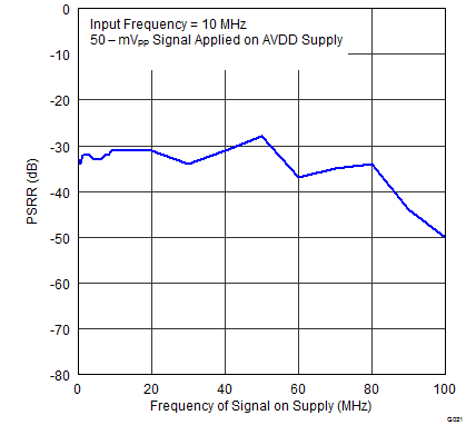 Figure 28. PSRR vs Frequency
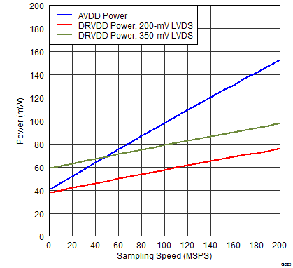 Figure 30. Power vs Sampling Frequency
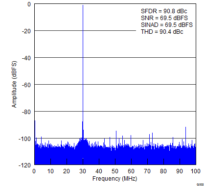 Figure 9. FFT for 170-MHz Input Signal
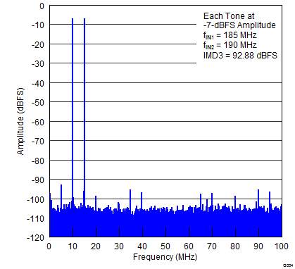 Figure 11. FFT for Two-Tone Input Signal
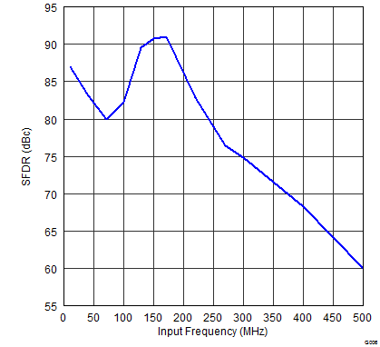 Figure 13. SFDR vs Input Frequency
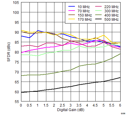 Figure 15. SFDR vs Digital Gain
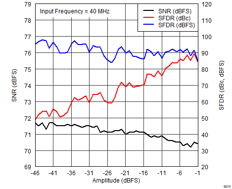 Figure 17. Performance Across Input Amplitude
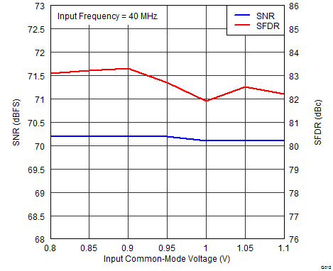 Figure 19. Performance vs Input Common-Mode Voltage
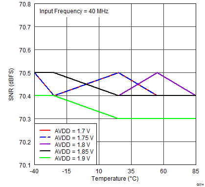 Figure 21. SNR vs AVDD Supply and Temperature
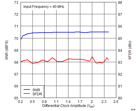 Figure 23. Performance vs Clock Amplitude
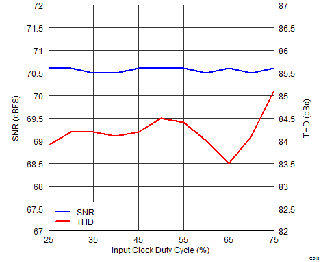 Figure 25. Performance vs Clock Duty Cycle
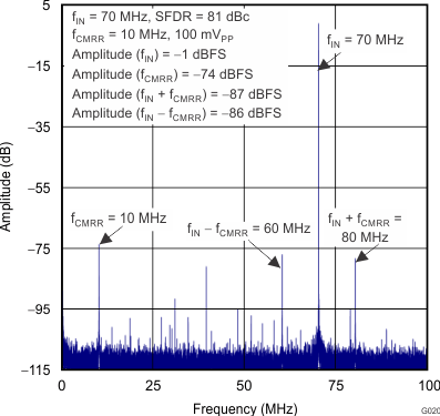 Figure 27. CMRR Spectrum
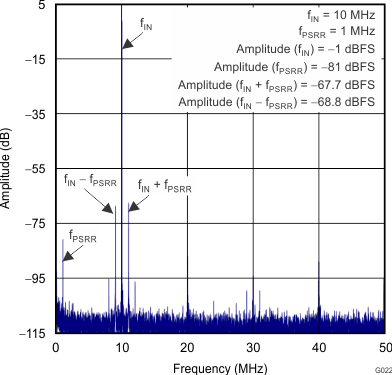 Figure 29. Zoomed View of Spectrum With PSRR Signal
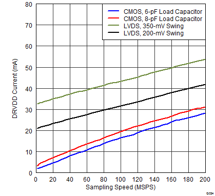 Figure 31. DRVDD Current vs Sampling Frequency
7.11 Typical Characteristics: Contour
At 25°C, AVDD = 1.8 V, DRVDD = 1.8 V, maximum rated sampling frequency, sine wave input clock, 1.5-VPP differential clock amplitude, 50% clock duty cycle, –1-dBFS differential analog input, 0-dB gain, low-latency mode, DDR LVDS output interface, and 32k-point FFT, unless otherwise noted.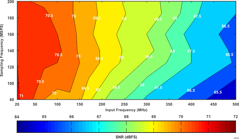 Figure 32. Signal-to-Noise Ratio (0-dB Gain)
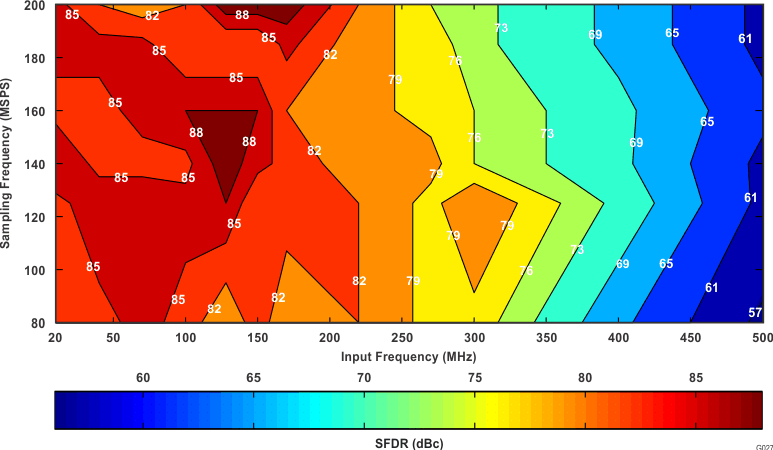 Figure 34. Spurious-Free Dynamic Range (0-dB Gain)
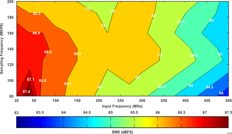 Figure 33. Signal-to-Noise Ratio (6-dB Gain)
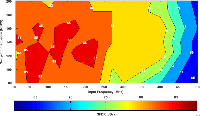 Figure 35. Spurious-Free Dynamic Range (6-dB Gain)