SBAS486F November 2009 – February 2016 ADS41B29 , ADS41B49
PRODUCTION DATA.
- 1 Features
- 2 Applications
- 3 Description
- 4 Revision History
- 5 Pin Configuration and Functions
-
6 Specifications
- 6.1 Absolute Maximum Ratings
- 6.2 ESD Ratings
- 6.3 Recommended Operating Conditions
- 6.4 Thermal Information
- 6.5 Electrical Characteristics: General
- 6.6 Electrical Characteristics: ADS41B29, ADS41B49
- 6.7 Digital Characteristics
- 6.8 Timing Requirements: LVDS and CMOS Modes
- 6.9 Timing Requirements: Reset
- 6.10 Timing Requirements: LVDS Timing Across Sampling Frequencies
- 6.11 Timing Requirements: CMOS Timing Across Sampling Frequencies
- 6.12 Timing Requirements: CMOS Timing Across Sampling Frequencies
- 6.13 Typical Characteristics: ADS41B49
- 6.14 Typical Characteristics: ADS41B29
- 6.15 Typical Characteristics: General
- 6.16 Typical Characteristics: Contour
- 7 Parameter Measurement Information
-
8 Detailed Description
- 8.1 Overview
- 8.2 Functional Block Diagram
- 8.3 Feature Description
- 8.4 Device Functional Modes
- 8.5 Programming
- 8.6
Register Maps
- 8.6.1
Serial Register Map
- 8.6.1.1 Summary of High-Performance Modes
- 8.6.1.2
Description of Serial Registers
- 8.6.1.2.1 Register Address 00h (address = 00h) [reset = 00h]
- 8.6.1.2.2 Register Address 01h (address = 01h) [reset = 00h]
- 8.6.1.2.3 Register Address 03h (address = 03h) [reset = 00h]
- 8.6.1.2.4 Register Address 25h (address = 25h) [reset = 50h]
- 8.6.1.2.5 Register Address 26h (address = 26h) [reset = 00h]
- 8.6.1.2.6 Register Address 3Dh (address = 3Dh) [reset = 00h]
- 8.6.1.2.7 Register Address 3Fh (address = 3Fh) [reset = 00h]
- 8.6.1.2.8 Register Address 40h (address = 40h) [reset = 00h]
- 8.6.1.2.9 Register Address 41h (address = 41h) [reset = 00h]
- 8.6.1.2.10 Register Address 42h (address = 42h) [reset = 08h]
- 8.6.1.2.11 Register Address 43h (address = 43h) [reset = 00h]
- 8.6.1.2.12 Register Address 4Ah (address = 4Ah) [reset = 00h]
- 8.6.1.2.13 Register Address BFh (address = BFh) [reset = 00h]
- 8.6.1.2.14 Register Address CFh (address = CFh) [reset = 00h]
- 8.6.1.2.15 Register Address DFh (address = DFh) [reset = 00h]
- 8.6.1
Serial Register Map
- 9 Application and Implementation
- 10Power Supply Recommendations
- 11Layout
- 12Device and Documentation Support
- 13Mechanical, Packaging, and Orderable Information
6 Specifications
6.1 Absolute Maximum Ratings(1)
| MIN | MAX | UNIT | ||
|---|---|---|---|---|
| Supply voltage range, AVDD | –0.3 | 2.1 | V | |
| Supply voltage range, AVDD_BUF | –0.3 | 3.9 | V | |
| Supply voltage range, DRVDD | –0.3 | 2.1 | V | |
| Voltage between AGND and DRGND | –0.3 | 0.3 | V | |
| Voltage between AVDD to DRVDD (when AVDD leads DRVDD) | –2.4 | 2.4 | V | |
| Voltage between DRVDD to AVDD (when DRVDD leads AVDD) | –2.4 | 2.4 | V | |
| Voltage between AVDD_BUF to DRVDD, AVDD | –4.2 | 4.2 | V | |
| Voltage applied to input pins | INP, INM | –0.3 | Minimum (1.9, AVDD + 0.3) |
V |
| CLKP, CLKM(2) | –0.3 | AVDD + 0.3 | ||
| RESET, SCLK, SDATA, SEN, DFS | –0.3 | 3.6 | ||
| Temperature | Operating free-air, TA | –40 | 125 | °C |
| Operating junction, TJ | 150 | |||
| Storage, Tstg | –65 | 150 | ||
(1) Stresses beyond those listed under Absolute Maximum Ratings may cause permanent damage to the device. These are stress ratings only, which do not imply functional operation of the device at these or any other conditions beyond those indicated under Recommended Operating Conditions. Exposure to absolute-maximum-rated conditions for extended periods may affect device reliability.
(2) When AVDD is turned off, switching off the input clock (or ensuring the voltage on CLKP, CLKM is less than |0.3 V|) is recommended. Doing so prevents the ESD protection diodes at the clock input pins from turning on.
6.2 ESD Ratings
| VALUE | UNIT | |||
|---|---|---|---|---|
| V(ESD) | Electrostatic discharge | Human-body model (HBM), per ANSI/ESDA/JEDEC JS-001(1) | ±2000 | V |
(1) JEDEC document JEP155 states that 500-V HBM allows safe manufacturing with a standard ESD control process.
6.3 Recommended Operating Conditions
| MIN | NOM | MAX | UNIT | |||
|---|---|---|---|---|---|---|
| SUPPLIES | ||||||
| AVDD | Analog supply voltage | 1.7 | 1.8 | 1.9 | V | |
| AVDD_BUF | Analog buffer supply voltage | 3 | 3.3 | 3.6 | V | |
| DRVDD | Digital supply voltage | 1.7 | 1.8 | 1.9 | V | |
| ANALOG INPUTS | ||||||
| Differential input voltage range(2) | 1.5 | VPP | ||||
| Input common-mode voltage | 1.7 ± 0.05 | V | ||||
| Maximum analog input frequency with 1.5-VPP input amplitude(1) | 400 | MHz | ||||
| Maximum analog input frequency with 1-VPP input amplitude(1) | 600 | MHz | ||||
| CLOCK INPUT | ||||||
| Low-speed mode enabled(3) | 20 | 80 | MSPS | |||
| Low-speed mode disabled(3) | > 80 | 250 | MSPS | |||
| Input clock amplitude differential (VCLKP – VCLKM) | ||||||
| Sine wave, ac-coupled | 0.2 | 1.5 | VPP | |||
| LVPECL, ac-coupled | 1.6 | VPP | ||||
| LVDS, ac-coupled | 0.7 | VPP | ||||
| LVCMOS, single-ended, ac-coupled | 1.8 | V | ||||
| Input clock duty cycle | Low-speed mode enabled | 40% | 50% | 60% | ||
| Low-speed mode disabled | 35% | 50% | 65% | |||
| DIGITAL OUTPUTS | ||||||
| CLOAD | Maximum external load capacitance from each output pin to DRGND | 5 | pF | |||
| RLOAD | Differential load resistance between the LVDS output pairs (LVDS mode) | 100 | Ω | |||
| TJ | Operating junction temperature | Recommended | 108 | °C | ||
| Maximum rated(7) | 125 | |||||
(1) See the Overview section in the Detailed Description.
(2) With 0-dB gain. See the Gain for SFDR, SNR Trade-Off section in Feature Description for the relationship between input voltage range and gain.
(3) See the Serial Interface section for details on the low-speed mode.
(4) Using these modes is recommended to get best performance. These modes can only be set with the serial interface.
(5) See the Serial Interface section for details on register programming.
(6) Note that these modes cannot be set when the serial interface is not used (when the RESET pin is tied high); see the Device Configuration section.
(7) Prolonged use at this junction temperature can increase the device failure-in-time (FIT) rate.
6.4 Thermal Information
| THERMAL METRIC(1) | ADS41B29, ADS41B49 | UNIT | |
|---|---|---|---|
| RGZ (VQFN) | |||
| 48 PINS | |||
| RθJA | Junction-to-ambient thermal resistance | 27.9 | °C/W |
| RθJC(top) | Junction-to-case (top) thermal resistance | 15.1 | °C/W |
| RθJB | Junction-to-board thermal resistance | 5.4 | °C/W |
| ψJT | Junction-to-top characterization parameter | 0.3 | °C/W |
| ψJB | Junction-to-board characterization parameter | 5.4 | °C/W |
| RθJC(bot) | Junction-to-case (bottom) thermal resistance | 1.7 | °C/W |
(1) For more information about traditional and new thermal metrics, see the Semiconductor and IC Package Thermal Metrics application report, SPRA953.
6.5 Electrical Characteristics: General
Typical values are at TA = 25°C, AVDD = 1.8 V, AVDD_BUF = 3.3 V, DRVDD = 1.8 V, and 50% clock duty cycle, unless otherwise noted. Minimum and maximum values are across the full ambient temperature range: TA, MIN = –40°C to TA, MAX = 85°C, AVDD = 1.8 V, AVDD_BUF = 3.3 V, and DRVDD = 1.8 V, unless otherwise noted.(3)| PARAMETER | TEST CONDITIONS | MIN | TYP | MAX | UNIT | |
|---|---|---|---|---|---|---|
| ANALOG INPUTS | ||||||
| Differential input voltage range | 1.5 | VPP | ||||
| Differential input resistance | At dc (see Figure 83) | 10 | kΩ | |||
| Differential input capacitance (see Figure 84) |
3.5 | pF | ||||
| Analog input bandwidth | 800 | MHz | ||||
| Analog input common-mode current (per input pin) |
2 | µA | ||||
| VCM | Common-mode output voltage | 1.7 | V | |||
| VCM output current capability | 4 | mA | ||||
| DC ACCURACY | ||||||
| Offset error | –15 | 2.5 | 15 | mV | ||
| Temperature coefficient of offset error | 0.003 | mV/°C | ||||
| EGREF | Gain error as a result of internal reference inaccuracy alone |
–2 | 2 | %FS | ||
| EGCHAN | Gain error of channel alone | 2.5 | %FS | |||
| POWER SUPPLY | ||||||
| IAVDD | Analog supply current | 99.5 | 115 | mA | ||
| IAVDD_BUF | Analog input buffer supply current | 29 | 42 | mA | ||
| IDRVDD | Output buffer supply current(2) | LVDS interface with 100-Ω external termination, low LVDS swing (200 mV) | 63 | mA | ||
| LVDS interface with 100-Ω external termination, standard LVDS swing (350 mV) |
75 | 90 | ||||
| IDRVDD output buffer supply current(2)(1) | CMOS interface(1), 8-pF external load capacitance, fIN = 2.5 MHz | 35 | mA | |||
| Global power-down | 10 | 25 | mW | |||
| Standby | 200 | mW | ||||
(1) In CMOS mode, the DRVDD current scales with the sampling frequency, the load capacitance on output pins, input frequency, and the supply voltage (see the CMOS Interface Power Dissipation section in the Feature Description).
(2) The maximum DRVDD current with CMOS interface depends on the actual load capacitance on the digital output lines. Note that the maximum recommended load capacitance on each digital output line is 10 pF.
(3) Minimum values for ADS41B49 are specified across the ambient temperature range of –40°C to +105°C.
6.6 Electrical Characteristics: ADS41B29, ADS41B49
Typical values are at TA = 25°C, AVDD = 1.8 V, AVDD_BUF = 3.3 V, DRVDD = 1.8 V, 1.5-VPP clock amplitude, 50% clock duty cycle, –1-dBFS differential analog input, and DDR LVDS interface, unless otherwise noted. Minimum and maximum values are across the full ambient temperature range: TA, MIN = –40°C to TA, MAX = 85°C, AVDD = 1.8 V, AVDD_BUF = 3.3 V, and DRVDD = 1.8 V, unless otherwise noted.| PARAMETER | TEST CONDITIONS | ADS41B29 | ADS41B49(1) | UNIT | |||||
|---|---|---|---|---|---|---|---|---|---|
| MIN | TYP | MAX | MIN | TYP | MAX | ||||
| Resolution | 12 | 14 | Bits | ||||||
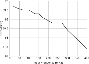
| SNR | Signal-to-noise ratio, LVDS | fIN = 20 MHz | 68.4 | 69.7 | dBFS | ||||
| fIN = 70 MHz | 68.3 | 69.5 | |||||||
| fIN = 100 MHz | 68.3 | 69.5 | |||||||
| fIN = 170 MHz | 65.5 | 68 | 66.5 | 69.1 | |||||
| fIN = 300 MHz | 67.5 | 68.4 | |||||||
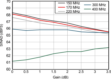
| SINAD | Signal-to-noise and distortion ratio, LVDS | fIN = 20 MHz | 68.3 | 69.5 | dBFS | ||||
| fIN = 70 MHz | 68.1 | 69.3 | |||||||
| fIN = 100 MHz | 68.2 | 69.3 | |||||||
| fIN = 170 MHz | 65 | 67.8 | 66 | 68.8 | |||||
| fIN = 300 MHz | 66.5 | 67.4 | |||||||
| SFDR | Spurious-free dynamic range | fIN = 20 MHz | 89 | 89 | dBc | ||||
| fIN = 70 MHz | 85 | 85 | |||||||
| fIN = 100 MHz | 87 | 87 | |||||||
| fIN = 170 MHz | 71 | 82 | 72 | 82 | |||||
| fIN = 300 MHz | 75 | 75 | |||||||
| THD | Total harmonic distortion | fIN = 20 MHz | 85 | 85 | dBc | ||||
| fIN = 70 MHz | 82 | 82 | |||||||
| fIN = 100 MHz | 83 | 83 | |||||||
| fIN = 170 MHz | 68 | 79.5 | 69 | 79.5 | |||||
| fIN = 300 MHz | 72 | 72 | |||||||
| HD2 | Second-order harmonic distortion | fIN = 20 MHz | 93 | 93 | dBc | ||||
| fIN = 70 MHz | 85 | 85 | |||||||
| fIN = 100 MHz | 87 | 87 | |||||||
| fIN = 170 MHz | 71 | 87 | 72 | 87 | |||||
| fIN = 300 MHz | 80 | 80 | |||||||
| HD3 | Third-order harmonic distortion | fIN = 20 MHz | 93 | 93 | dBc | ||||
| fIN = 70 MHz | 88 | 88 | |||||||
| fIN = 100 MHz | 88 | 88 | |||||||
| fIN = 170 MHz | 71 | 82 | 72 | 82 | |||||
| fIN = 300 MHz | 75 | 75 | |||||||
| Worst spur (other than second- and third-order harmonics) |
fIN = 20 MHz | 89 | 89 | dBc | |||||
| fIN = 70 MHz | 90 | 90 | |||||||
| fIN = 100 MHz | 90 | 90 | |||||||
| fIN = 170 MHz | 76 | 88 | 77.5 | 88 | |||||
| fIN = 300 MHz | 88 | 88 | |||||||
| IMD | Two-tone intermodulation distortion | f1 = 185 MHz, f2 = 190 MHz, each tone at –7 dBFS |
–86 | –86 | dBFS | ||||
| Input overload recovery | Recovery to within 1% (of final value) for 6-dB overload with sine-wave input | 1 | 1 | Clock cycles | |||||
| PSRR | AC power-supply rejection ratio | For 100-mVPP signal on AVDD supply, up to 10 MHz | > 30 | > 30 | dB | ||||
| ENOB | Effective number of bits | fIN = 170 MHz | 11 | 11.2 | LSBs | ||||
| INL | Integrated nonlinearity | fIN = 170 MHz | ±1.5 | ±3.5 | ±2.5 | ±5 | LSBs | ||
(1) Minimum values for the ADS41B49 are specified across the ambient temperature range of –40°C to +105°C.
6.7 Digital Characteristics(4)
Typical values are at TA = 25°C, AVDD = 1.8 V, AVDD_BUF = 3.3 V, and DRVDD = 1.8 V, unless otherwise noted. Minimum and maximum values are across the full ambient temperature range: TA, MIN = –40°C to TA, MAX = 85°C, AVDD = 1.8 V, AVDD_BUF = 3.3 V, and DRVDD = 1.8 V.| PARAMETER | TEST CONDITIONS | MIN | TYP | MAX | UNIT | ||
|---|---|---|---|---|---|---|---|
| DIGITAL INPUTS (RESET, SCLK, SDATA, SEN, OE) | |||||||
| High-level input voltage | RESET, SCLK, SDATA, and SEN support 1.8-V and 3.3-V CMOS logic levels | 1.3 | V | ||||
| OE only supports 1.8-V CMOS logic levels | 1.3 | V | |||||
| Low-level input voltage | RESET, SCLK, SDATA, and SEN support 1.8-V and 3.3-V CMOS logic levels | 0.4 | V | ||||
| OE only supports 1.8-V CMOS logic levels | 0.4 | V | |||||
| High-level input current | SDATA, SCLK(1) | VHIGH = 1.8 V | 10 | µA | |||
| SEN(3) | VHIGH = 1.8 V | 0 | µA | ||||
| Low-level input current | SDATA, SCLK | VLOW = 0 V | 0 | µA | |||
| SEN | VLOW = 0 V | –10 | µA | ||||
| DIGITAL OUTPUTS (CMOS INTERFACE: D0 TO D13, OVR_SDOUT) | |||||||
| High-level output voltage | DRVDD – 0.1 | DRVDD | V | ||||
| Low-level output voltage | 0 | 0.1 | V | ||||
| DIGITAL OUTPUTS (LVDS INTERFACE: D0_D1_P/M to D12_D13_P/M, CLKOUTP/M) | |||||||
| VODH | High-level output voltage(2) | Standard swing LVDS | 270 | 350 | 430 | mV | |
| Low swing LVDS | 200 | mV | |||||
| VODL | Low-level output voltage(2) | Standard swing LVDS | –430 | –350 | –270 | mV | |
| Low swing LVDS | –200 | mV | |||||
| VOCM | Output common-mode voltage | 0.85 | 1.05 | 1.25 | V | ||
(1) SDATA and SCLK have an internal 180-kΩ pull-down resistor.
(2) With an external 100-Ω termination.
(3) SEN has an internal 180-kΩ pull-up resistor to AVDD.
(4) Minimum values for ADS41B49 are specified across the ambient temperature range of –40°C to +105°C.
6.8 Timing Requirements: LVDS and CMOS Modes
Typical values are at TA = 25°C, AVDD = 1.8 V, AVDD_BUF = 3.3 V, DRVDD = 1.8 V, sampling frequency = 250 MSPS, sine-wave input clock, CLOAD = 5 pF(2), and RLOAD = 100 Ω(3), unless otherwise noted. Minimum and maximum values are across the full ambient temperature range: TA, MIN = –40°C to TA, MAX = 85°C, AVDD = 1.8 V, AVDD_BUF = 3.3 V, and DRVDD = 1.7 V to 1.9 V.(1)| MIN | TYP | MAX | UNIT | |||
|---|---|---|---|---|---|---|
| GENERAL | ||||||
| tA | Aperture delay | 0.6 | 0.8 | 1.2 | ns | |
| Variation of aperture delay between two devices at the same temperature and DRVDD supply | ±100 | ps | ||||
| tJ | Aperture jitter | 100 | fS rms | |||
| Wakeup time | Time to valid data after coming out of STANDBY mode | 5 | 25 | µs | ||
| Time to valid data after coming out of PDN GLOBAL mode | 100 | 500 | ||||
| ADC latency(6) | Gain enabled (default after reset) | 21 | Clock cycles | |||
| Gain and offset correction enabled | 22 | |||||
| DDR LVDS MODE | ||||||
| tSU | Data setup time(3): data valid(4) to zero-crossing of CLKOUTP | 0.75(7) | 1.1 | ns | ||
| tH | Data hold time(3): zero-crossing of CLKOUTP to data becoming invalid(4) | 0.35(8) | 0.6 | ns | ||
| tPDI | Clock propagation delay: input clock rising edge cross-over to output clock rising edge cross-over, 1 MSPS ≤ sampling frequency ≤ 250 MSPS | 3 | 4.2 | 5.4 | ns | |
| Variation of tPDI between two devices at the same temperature and DRVDD supply | ±0.6 | ns | ||||
| LVDS bit clock duty cycle of differential clock, (CLKOUTP – CLKOUTM), 1 MSPS ≤ sampling frequency ≤ 250 MSPS |
42% | 48% | 54% | |||
| tRISE, tFALL | Data rise and fall time: rise time measured from –100 mV to +100 mV, fall time measured from +100 mV to –100 mV, 1 MSPS ≤ sampling frequency ≤ 250 MSPS | 0.14 | ns | |||
| tCLKRISE, tCLKFALL |
Output clock rise and fall time: rise time measured from –100 mV to +100 mV, fall time measured from +100 mV to –100 mV, 1 MSPS ≤ sampling frequency ≤ 250 MSPS | 0.14 | ns | |||
| tOE | Output enable (OE) to data delay time to valid data after OE becomes active | 50 | 100 | ns | ||
| PARALLEL CMOS MODE(5) | ||||||
| tSTART | Input clock to data delay: input clock rising edge cross-over to start of data valid(4) | 1.6 | ns | |||
| tDV | Data valid time interval of valid data(4) | 2.5 | 3.2 | ns | ||
| tPDI | Clock propagation delay: input clock rising edge cross-over to, output clock rising edge cross-over, 1 MSPS ≤ sampling frequency ≤ 200 MSPS | 4 | 5.5 | 7 | ns | |
| Output clock duty cycle of output clock (CLKOUT), 1 MSPS ≤ sampling frequency ≤ 200 MSPS |
47% | |||||
| tRISE, tFALL | Data rise and fall time: rise time measured from 20% to 80% of DRVDD, fall time measured from 80% to 20% of DRVDD, 1 MSPS ≤ sampling frequency ≤ 250 MSPS | 0.35 | ns | |||
| tCLKRISE, tCLKFALL |
Output clock rise and fall time: rise time measured from 20% to 80% of DRVDD, fall time measured from 80% to 20% of DRVDD, 1 MSPS ≤ sampling frequency ≤ 200 MSPS |
0.35 | ns | |||
| tOE | Output enable (OE) to data delay time to valid data after OE becomes active | 20 | 40 | ns | ||
(1) Timing parameters are ensured by design and characterization but are not production tested.
(2) CLOAD is the effective external single-ended load capacitance between each output pin and ground.
(3) RLOAD is the differential load resistance between the LVDS output pair.
(4) Data valid refers to a logic high of 1.26 V and a logic low of 0.54 V.
(5) For fS > 200 MSPS, using an external clock is recommended for data capture instead of the device output clock signal (CLKOUT).
(6) At higher frequencies, tPDI is greater than one clock period and overall latency = ADC latency + 1.
(7) For an ambient temperature range of –40°C to +105°C, the minimum value of setup time reduces to 0.7 ns.
(8) For an ambient temperature range of –40°C to +105°C, the minimum value of setup time reduces to 0.3 ns.
6.9 Timing Requirements: Reset
Typical values at TA = 25°C and minimum and maximum values across the full ambient temperature range: TA, MIN = –40°C to TA, MAX = 85°C, unless otherwise noted.(2)| MIN | TYP | MAX | UNIT | ||
|---|---|---|---|---|---|
| t1 | Power-on delay from power-up of AVDD and DRVDD to RESET pulse active | 1 | ms | ||
| t2 | Reset pulse duration of active RESET signal that resets the serial registers | 10 | ns | ||
| 1(1) | µs | ||||
| t3 | Delay from RESET disable to SEN active | 100 | ns | ||
(1) The reset pulse is needed only when using the serial interface configuration. If the pulse width is greater than 1 µs, the device could enter the parallel configuration mode briefly and then return back to serial interface mode.
(2) For the ADS41B49, the minimum and maximum values are given for the ambient temperature range of TA, MIN = –40°C to TA, MAX = 105°C.
6.10 Timing Requirements: LVDS Timing Across Sampling Frequencies
| SAMPLING FREQUENCY (MSPS) | SETUP TIME (ns) | HOLD TIME (ns) | ||||
|---|---|---|---|---|---|---|
| MIN | TYP | MAX | MIN | TYP | MAX | |
| 230 | 0.85 | 1.25 | 0.35 | 0.6 | ||
| 200 | 1.05 | 1.55 | 0.35 | 0.6 | ||
| 185 | 1.1 | 1.7 | 0.35 | 0.6 | ||
| 160 | 1.6 | 2.1 | 0.35 | 0.6 | ||
| 125 | 2.3 | 3 | 0.35 | 0.6 | ||
| 80 | 4.5 | 5.2 | 0.35 | 0.6 | ||
6.11 Timing Requirements: CMOS Timing Across Sampling Frequencies
| SAMPLING FREQUENCY (MSPS) | TIMING SPECIFIED WITH RESPECT TO OUTPUT CLOCK | ||||||||
|---|---|---|---|---|---|---|---|---|---|
| tSETUP (ns) | tHOLD (ns) | tPDI (ns) | |||||||
| MIN | TYP | MAX | MIN | TYP | MAX | MIN | TYP | MAX | |
| 200 | 1 | 1.6 | 2 | 2.8 | 4 | 5.5 | 7 | ||
| 185 | 1.3 | 2 | 2.2 | 3 | 4 | 5.5 | 7 | ||
| 160 | 1.8 | 2.5 | 2.5 | 3.3 | 4 | 5.5 | 7 | ||
| 125 | 2.5 | 3.2 | 3.5 | 4.3 | 4 | 5.5 | 7 | ||
| 80 | 4.8 | 5.5 | 5.7 | 6.5 | 4 | 5.5 | 7 | ||
6.12 Timing Requirements: CMOS Timing Across Sampling Frequencies
| SAMPLING FREQUENCY (MSPS) | TIMING SPECIFIED WITH RESPECT TO INPUT CLOCK | |||||
|---|---|---|---|---|---|---|
| tSTART (ns) | tDV (ns) | |||||
| MIN | TYP | MAX | MIN | TYP | MAX | |
| 250 | 1.6 | 2.5 | 3.2 | |||
| 230 | 1.1 | 2.9 | 3.5 | |||
| 200 | 0.3 | 3.5 | 4.2 | |||
| 185 | 0 | 3.9 | 4.5 | |||
| 170 | –1.3 | 4.3 | 5 | |||
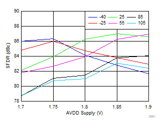
6.13 Typical Characteristics: ADS41B49
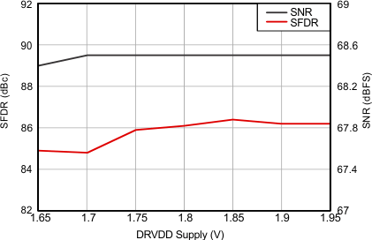
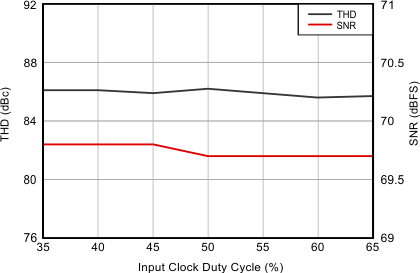
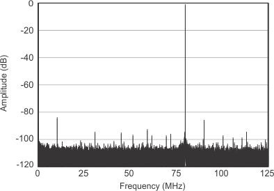
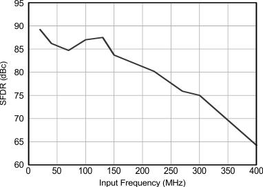
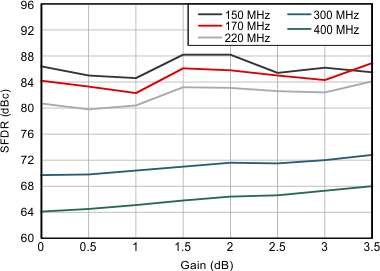
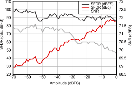
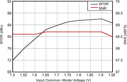
At 25°C, AVDD = 1.8 V, AVDD_BUF = 3.3 V, DRVDD = 1.8 V, maximum-rated sampling frequency, sine wave input clock, 1.5-VPP differential clock amplitude, 50% clock duty cycle, –1-dBFS differential analog input, DDR LVDS output interface, and 32k-point FFT, unless otherwise noted.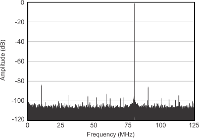
| SFDR = 90.3 dBc, SNR = 69.9 dBFS, SINAD = 69.8 dBFS, THD = 85.2 dBc |
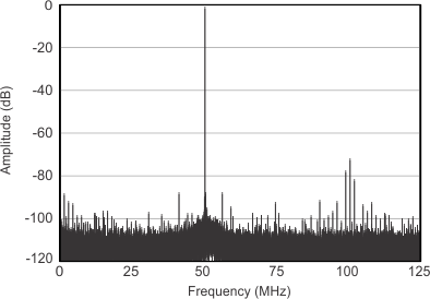
| SFDR = 70.7 dBc, SNR = 68.4 dBFS, SINAD = 66.3 dBFS, THD = 69.3 dBc |
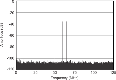
| Each tone at –36-dBFS amplitude, fIN1 = 185 MHz, fIN2 = 190 MHz, two-tone IMD = 89.7 dBFS, SFDR = 106.4 dBFS |
| Input frequency = 170 MHz |
(Single Tone)
| Input frequency = 170 MHz |
| Input frequency = 10 MHz |
| SFDR = 82.9 dBc, SNR = 69.3 dBFS, SINAD = 69 dBFS, THD = 80.3 dBc |
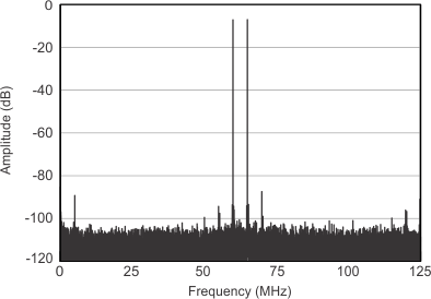
| Each tone at –7-dBFS amplitude, fIN1 = 185 MHz, fIN2 = 190 MHz, two-tone IMD = 87.3 dBFS, SFDR = 96.0 dBFS |
| Input frequency = 40 MHz |
(Single Tone)
| Input frequency = 170 MHz |
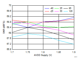
| Input frequency = 170 MHz |
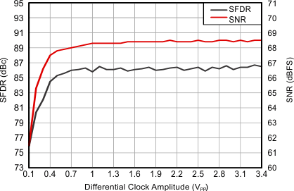
| Input frequency = 170 MHz |
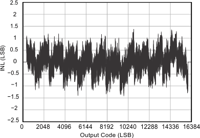
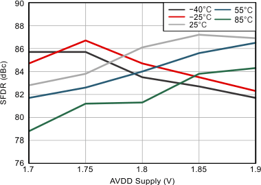
6.14 Typical Characteristics: ADS41B29
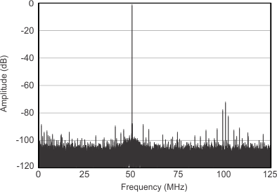
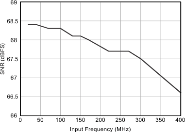
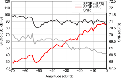
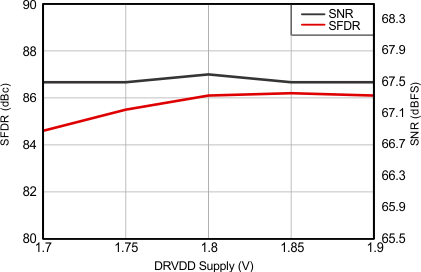
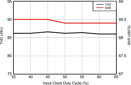
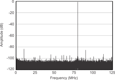
At 25°C, AVDD = 1.8 V, AVDD_BUF = 3.3 V, DRVDD = 1.8 V, maximum-rated sampling frequency, sine wave input clock, 1.5-VPP differential clock amplitude, 50% clock duty cycle, –1-dBFS differential analog input, DDR LVDS output interface, and 32k-point FFT, unless otherwise noted.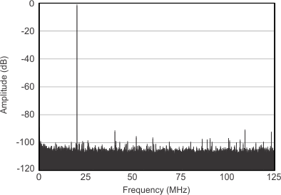
| SFDR = 89.6 dBc, SNR = 68.6 dBFS, SINAD = 68.5 dBFS, THD = 85.2 dBc |
| SFDR = 70.8 dBc, SNR = 67.4 dBFS, SINAD = 65.7 dBFS, THD = 69.4 dBc |
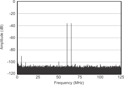
| Each tone at –36-dBFS amplitude, fIN1 = 185 MHz, fIN2 = 190 MHz, two-tone IMD = 89.8 dBFS, SFDR = 98.5 dBFS |

| Input frequency = 40 MHz |
(Single Tone)
| Input frequency = 170 MHz |
| Input frequency = 10 MHz |
| SFDR = 82.3 dBc, SNR = 68.1 dBFS, SINAD = 67.8 dBFS, THD = 79.9 dBc |
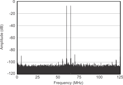
| Each tone at –7-dBFS amplitude, fIN1 = 185 MHz, fIN2 = 190 MHz, two-tone IMD = 87.3 dBFS, SFDR = 85.9 dBFS |

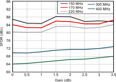
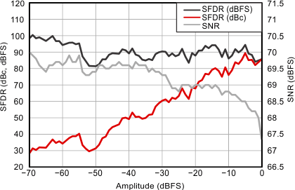
| Input frequency = 170 MHz |
(Single Tone)
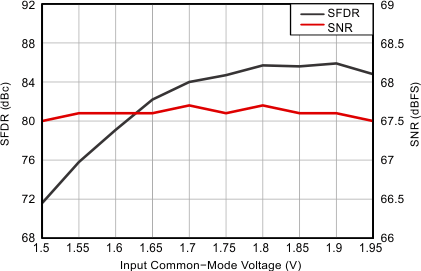
| Input frequency = 170 MHz |
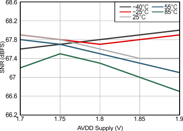
| Input frequency = 170 MHz |
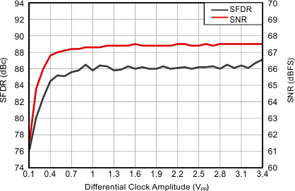
| Input frequency = 170 MHz |
6.15 Typical Characteristics: General
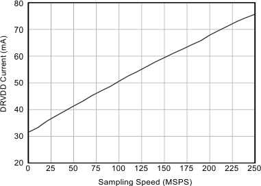
At 25°C, AVDD = 1.8 V, AVDD_BUF = 3.3 V, DRVDD = 1.8 V, maximum-rated sampling frequency, sine wave input clock, 1.5-VPP differential clock amplitude, 50% clock duty cycle, –1-dBFS differential analog input, DDR LVDS output interface, and 32k-point FFT, unless otherwise noted.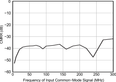
| Input frequency = 170 MHz, 50-mVPP signal superimposed on input common-mode voltage (1.7 V) | ||
|
|
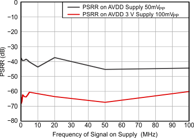
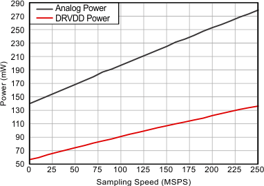
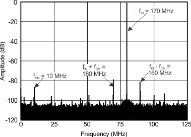
| fIN = 170 MHz; fCM = 10 MHz, 50 mVPP; SFDR = 77.69 dB; amplitude: (fIN) = –1 dBFS; (fCM) = –93.8 dBFS; (fIN + fCM) = –78.8 dBFS; (fIN – fCM) = –81 dBFS |
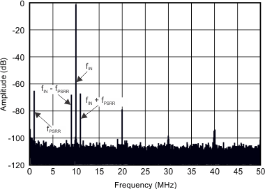
| fIN = 10 MHz; fPSRR = 10 MHz, 50 mVPP; amplitude: (fIN) = –1 dBFS; (fPSRR) = –65.6 dBFS; (fIN + fPSRR) = –67.5 dBFS; (fIN – fPSRR) = –68.3 dBFS |
6.16 Typical Characteristics: Contour
At 25°C, AVDD = 1.8 V, AVDD_BUF = 3.3 V, DRVDD = 1.8 V, maximum-rated sampling frequency, sine wave input clock, 1.5-VPP differential clock amplitude, 50% clock duty cycle, –1-dBFS differential analog input, DDR LVDS output interface, and 32k-point FFT, unless otherwise noted.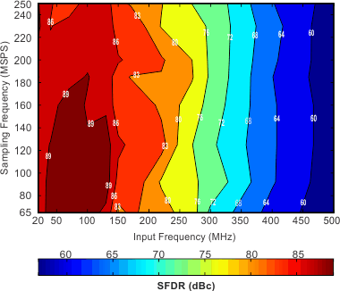
(0-dB Gain, Applies to ADS41Bx9)
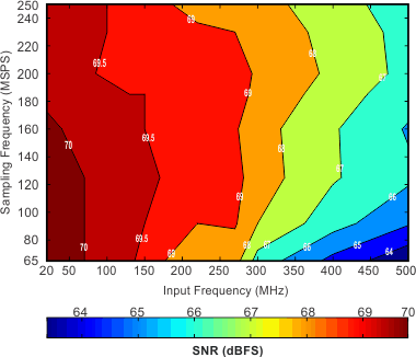
(0-dB Gain, Applies to ADS41B49)
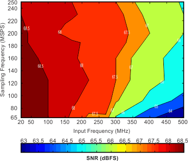
(0-dB Gain, Applies to ADS41B29)
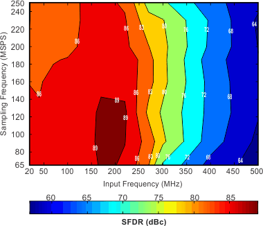
(3.5-dB Gain, Applies to ADS41Bx9)
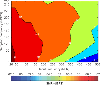
(3.5-dB Gain, Applies to ADS41B49)
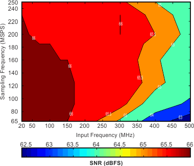
(0-dB Gain, Applies to ADS41B29)
