SBAS486F November 2009 – February 2016 ADS41B29 , ADS41B49
PRODUCTION DATA.
- 1 Features
- 2 Applications
- 3 Description
- 4 Revision History
- 5 Pin Configuration and Functions
-
6 Specifications
- 6.1 Absolute Maximum Ratings
- 6.2 ESD Ratings
- 6.3 Recommended Operating Conditions
- 6.4 Thermal Information
- 6.5 Electrical Characteristics: General
- 6.6 Electrical Characteristics: ADS41B29, ADS41B49
- 6.7 Digital Characteristics
- 6.8 Timing Requirements: LVDS and CMOS Modes
- 6.9 Timing Requirements: Reset
- 6.10 Timing Requirements: LVDS Timing Across Sampling Frequencies
- 6.11 Timing Requirements: CMOS Timing Across Sampling Frequencies
- 6.12 Timing Requirements: CMOS Timing Across Sampling Frequencies
- 6.13 Typical Characteristics: ADS41B49
- 6.14 Typical Characteristics: ADS41B29
- 6.15 Typical Characteristics: General
- 6.16 Typical Characteristics: Contour
- 7 Parameter Measurement Information
-
8 Detailed Description
- 8.1 Overview
- 8.2 Functional Block Diagram
- 8.3 Feature Description
- 8.4 Device Functional Modes
- 8.5 Programming
- 8.6
Register Maps
- 8.6.1
Serial Register Map
- 8.6.1.1 Summary of High-Performance Modes
- 8.6.1.2
Description of Serial Registers
- 8.6.1.2.1 Register Address 00h (address = 00h) [reset = 00h]
- 8.6.1.2.2 Register Address 01h (address = 01h) [reset = 00h]
- 8.6.1.2.3 Register Address 03h (address = 03h) [reset = 00h]
- 8.6.1.2.4 Register Address 25h (address = 25h) [reset = 50h]
- 8.6.1.2.5 Register Address 26h (address = 26h) [reset = 00h]
- 8.6.1.2.6 Register Address 3Dh (address = 3Dh) [reset = 00h]
- 8.6.1.2.7 Register Address 3Fh (address = 3Fh) [reset = 00h]
- 8.6.1.2.8 Register Address 40h (address = 40h) [reset = 00h]
- 8.6.1.2.9 Register Address 41h (address = 41h) [reset = 00h]
- 8.6.1.2.10 Register Address 42h (address = 42h) [reset = 08h]
- 8.6.1.2.11 Register Address 43h (address = 43h) [reset = 00h]
- 8.6.1.2.12 Register Address 4Ah (address = 4Ah) [reset = 00h]
- 8.6.1.2.13 Register Address BFh (address = BFh) [reset = 00h]
- 8.6.1.2.14 Register Address CFh (address = CFh) [reset = 00h]
- 8.6.1.2.15 Register Address DFh (address = DFh) [reset = 00h]
- 8.6.1
Serial Register Map
- 9 Application and Implementation
- 10Power Supply Recommendations
- 11Layout
- 12Device and Documentation Support
- 13Mechanical, Packaging, and Orderable Information
9 Application and Implementation
NOTE
Information in the following applications sections is not part of the TI component specification, and TI does not warrant its accuracy or completeness. TI’s customers are responsible for determining suitability of components for their purposes. Customers should validate and test their design implementation to confirm system functionality.
9.1 Application Information
9.1.1 Drive Circuit Requirements
For optimum performance, the analog inputs must be driven differentially. This technique improves the common-mode noise immunity and even-order harmonic rejection. A small resistor (5 Ω to 10 Ω) in series with each input pin is recommended to damp out ringing caused by package parasitics.
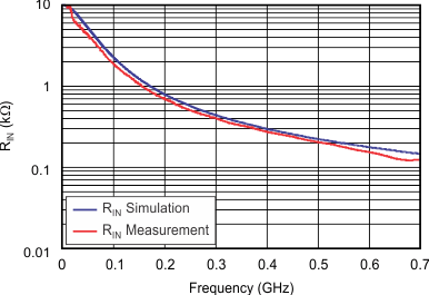
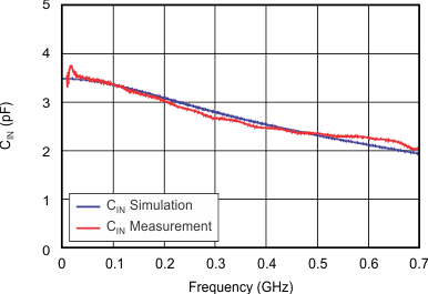
Figure 83 and Figure 84 show the differential impedance (ZIN = RIN || CIN) between the ADC analog input pins INP and INM. The presence of the analog input buffer results in an almost constant input capacitance up to 1 GHz.
9.1.2 Driving Circuit
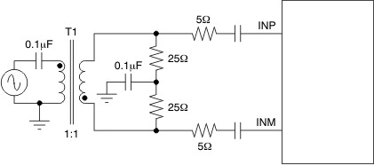
Two example driving circuit configurations are shown in Figure 85 and Figure 86—one optimized for low input frequencies and the other optimized for high input frequencies. Notice in both cases that the board circuitry is simplified compared to the non-buffered ADS4149.
In Figure 85, a single transformer is used and is suited for low input frequencies. To optimize even-harmonic performance at high input frequencies (greater than the first Nyquist), the use of back-to-back transformers is recommended (see Figure 86). Note that both drive circuits have been terminated by 50 Ω near the ADC side. The ac-coupling capacitors allow the analog inputs to self-bias around the required common-mode voltage.
 Figure 85. Drive Circuit for Low Input Frequencies
 Figure 86. Drive Circuit for High Input Frequencies
The mismatch in the transformer parasitic capacitance (between the windings) results in degraded even-order harmonic performance. Connecting two identical RF transformers back-to-back helps minimize this mismatch and good performance is obtained for high-frequency input signals. An additional termination resistor pair may be required between the two transformers, as shown in Figure 85 and Figure 86. The center point of this termination is connected to ground to improve the balance between the P (positive) and M (negative) sides. The values of the terminations between the transformers and on the secondary side must be chosen to obtain an effective 50 Ω (for a 50-Ω source impedance).

