ZHCS114E march 2011 – february 2023 ADS4222 , ADS4225 , ADS4226 , ADS4242 , ADS4245 , ADS4246
PRODUCTION DATA
- 1 特性
- 2 应用
- 3 说明
- 4 Revision History
- 5 说明(续)
- 6 Pin Configuration and Functions
-
7 Specifications
- 7.1 Absolute Maximum Ratings
- 7.2 ESD Ratings
- 7.3 Recommended Operating Conditions
- 7.4 Thermal Information
- 7.5 Electrical Characteristics: ADS4246, ADS4245, ADS4242
- 7.6 Electrical Characteristics: ADS4226, ADS4225, ADS4222
- 7.7 Electrical Characteristics: General
- 7.8 Digital Characteristics
- 7.9 Timing Requirements: LVDS and CMOS Modes #GUID-C6C0701B-A11B-492F-BD6B-B774F5FE4665/SLAS6895399
- 7.10 Serial Interface Timing Characteristics #GUID-3852E7CE-C5B6-42F5-A56A-70AB1B981302/SBAS5097810
- 7.11 Reset Timing (Only When Serial Interface Is Used)
- 7.12 Typical Characteristics
-
8 Detailed Description
- 8.1 Overview
- 8.2 Functional Block Diagrams
- 8.3 Feature Description
- 8.4 Device Functional Modes
- 8.5 Programming
- 8.6 Register Maps
- 9 Application and Implementation
- 10Device and Documentation Support
- 11Mechanical, Packaging, and Orderable Information
7.11 Reset Timing (Only When Serial Interface Is Used)
See the Serial Register Readout section.
| PARAMETER | CONDITIONS | MIN | TYP(1) | MAX | UNIT | |
|---|---|---|---|---|---|---|
| t1 | Power-on delay | Delay from AVDD and DRVDD power-up to active RESET pulse | 1 | ms | ||
| t2 | Reset pulse width | Active RESET signal pulse width | 10 | ns | ||
| 1 | µs | |||||
| t3 | Register write delay | Delay from RESET disable to SEN active | 100 | ns | ||
(1) Typical values at 25°C; minimum and maximum values across the
full temperature range: TMIN = –40°C to TMAX = 85°C,
unless otherwise noted.
Table 7-1 LVDS Timings at Lower Sampling
Frequencies
| SAMPLING FREQUENCY (MSPS) | SETUP TIME (ns) | HOLD TIME (ns) | tPDI, CLOCK PROPAGATION DELAY (ns) |
||||||
|---|---|---|---|---|---|---|---|---|---|
| MIN | TYP | MAX | MIN | TYP | MAX | MIN | TYP | MAX | |
| 65 | 5.9 | 6.6 | 0.35 | 0.6 | 5 | 6.1 | 7.5 | ||
| 80 | 4.5 | 5.2 | 0.35 | 0.6 | 5 | 6.1 | 7.5 | ||
| 105 | 3.1 | 3.6 | 0.35 | 0.6 | 5 | 6.1 | 7.5 | ||
| 125 | 2.3 | 2.9 | 0.35 | 0.6 | 5 | 6.1 | 7.5 | ||
| 150 | 1.7 | 2.2 | 0.35 | 0.6 | 5 | 6.1 | 7.5 | ||
Table 7-2 CMOS Timings at Lower Sampling
Frequencies
| SAMPLING FREQUENCY (MSPS) | TIMINGS SPECIFIED WITH RESPECT TO CLKOUT | ||||||||
|---|---|---|---|---|---|---|---|---|---|
| SETUP TIME (ns) | HOLD TIME (ns) | tPDI, CLOCK PROPAGATION DELAY (ns) |
|||||||
| MIN | TYP | MAX | MIN | TYP | MAX | MIN | TYP | MAX | |
| 65 | 6.1 | 7.2 | 6.7 | 7.1 | 4.5 | 6.4 | 8.5 | ||
| 80 | 4.7 | 5.8 | 5.3 | 5.8 | 4.5 | 6.4 | 8.5 | ||
| 105 | 3.4 | 4.3 | 3.8 | 4.3 | 4.5 | 6.4 | 8.5 | ||
| 125 | 2.7 | 3.6 | 3.1 | 3.6 | 4.5 | 6.4 | 8.5 | ||
| 150 | 1.9 | 2.8 | 2.5 | 2.9 | 4.5 | 6.4 | 8.5 | ||
Table 7-3 High-Performance Modes
| PARAMETER(1)(2) | DESCRIPTION |
|---|---|
| High-performance mode | Set the HIGH PERF MODE
register bit to obtain best performance across sample clock and
input signal frequencies. See Figure 7-5. Register address = 03h, data = 03h |
| High-frequency mode | Set the HIGH FREQ MODE CH
A and HIGH FREQ MODE CH B register bits for high input signal
frequencies greater than 200 MHz. See Figure 7-5. Register address = 4Ah, data = 01h Register address = 58h, data = 01h |
(1) It is recommended to use these modes to obtain best
performance.
(2) See the Serial Interface Configuration section for details on
register programming.

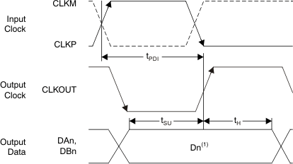
A. Dn = bits D0, D1, D2, etc. of
channels A and B.
Figure 7-1 CMOS
Interface Timing Diagram
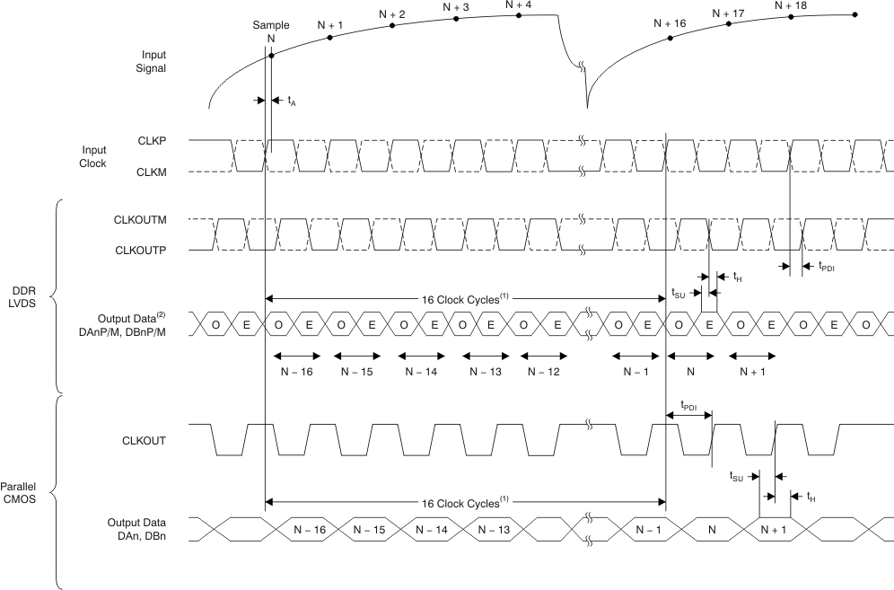
A. ADC latency after reset. At
higher sampling frequencies, tPDI is greater than one clock cycle,
which then makes the overall latency = ADC latency + 1.
B. E = even bits (D0, D2, D4, etc.);
O = odd bits (D1, D3, D5, etc.).
Figure 7-2 Latency
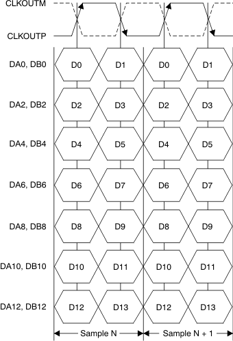
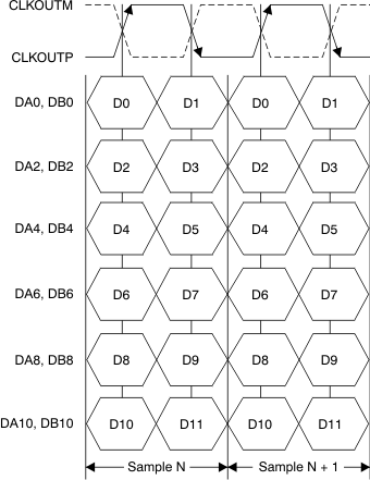
Timing Diagram Figure 7-3 ADS4246/45/42 LVDS Interface Timing Diagram
 Figure 7-4 ADS4226/25/22 LVDS Interface Timing Diagram
A. With external 100-Ω
termination.
Figure 7-5 LVDS
Output Voltage Levels