ZHCS171C June 2011 – May 2015 ADS4229
PRODUCTION DATA.
- 1 特性
- 2 应用
- 3 说明
- 4 修订历史记录
- 5 Device Comparison Table
- 6 Pin Configuration and Functions
-
7 Specifications
- 7.1 Absolute Maximum Ratings
- 7.2 ESD Ratings
- 7.3 Recommended Operating Conditions
- 7.4 Thermal Information
- 7.5 Electrical Characteristics: ADS4229 (250 MSPS)
- 7.6 Electrical Characteristics: General
- 7.7 Digital Characteristics
- 7.8 LVDS and CMOS Modes Timing Requirements
- 7.9 LVDS Timings at Lower Sampling Frequencies
- 7.10 CMOS Timings at Lower Sampling Frequencies
- 7.11 Serial Interface Timing Characteristics
- 7.12 Reset Timing (Only when Serial Interface is Used)
- 7.13 Typical Characteristics
-
8 Detailed Description
- 8.1 Overview
- 8.2 Functional Block Diagram
- 8.3 Feature Description
- 8.4 Device Functional Modes
- 8.5 Programming
- 8.6
Register Maps
- 8.6.1 Serial Register Map
- 8.6.2
Description of Serial Registers
- 8.6.2.1 Register Address 00h (Default = 00h)
- 8.6.2.2 Register Address 01h (Default = 00h)
- 8.6.2.3 Register Address 03h (Default = 00h)
- 8.6.2.4 Register Address 25h (Default = 00h)
- 8.6.2.5 Register Address 29h (Default = 00h)
- 8.6.2.6 Register Address 2Bh (Default = 00h)
- 8.6.2.7 Register Address 3Dh (Default = 00h)
- 8.6.2.8 Register Address 3Fh (Default = 00h)
- 8.6.2.9 Register Address 40h (Default = 00h)
- 8.6.2.10 Register Address 41h (Default = 00h)
- 8.6.2.11 Register Address 42h (Default = 00h)
- 8.6.2.12 Register Address 45h (Default = 00h)
- 8.6.2.13 Register Address 4Ah (Default = 00h)
- 8.6.2.14 Register Address 58h (Default = 00h)
- 8.6.2.15 Register Address BFh (Default = 00h)
- 8.6.2.16 Register Address C1h (Default = 00h)
- 8.6.2.17 Register Address CFh (Default = 00h)
- 8.6.2.18 Register Address EFh (Default = 00h)
- 8.6.2.19 Register Address F1h (Default = 00h)
- 8.6.2.20 Register Address F2h (Default = 00h)
- 8.6.2.21 Register Address 2h (Default = 00h)
- 8.6.2.22 Register Address D5h (Default = 00h)
- 8.6.2.23 Register Address D7h (Default = 00h)
- 8.6.2.24 Register Address DBh (Default = 00h)
- 9 Application and Implementation
- 10Power Supply Recommendations
- 11Layout
- 12器件和文档支持
- 13机械、封装和可订购信息
6 Pin Configuration and Functions
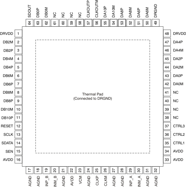
RGC Package (LVDS Mode)
64-Pin VQFN
Top View

1. The PowerPAD is connected to DRGND.
NOTE: NC = do not connect; must float.
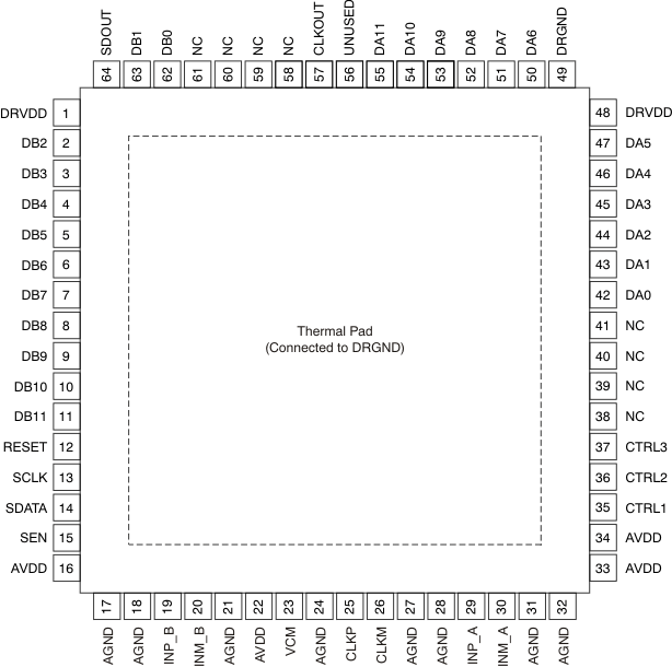
RGC Package (CMOS Mode)
64-Pin VQFN
Top View

Pin Functions (LVDS Mode)
| PIN | I/O | DESCRIPTION | |
|---|---|---|---|
| NAME | NO. | ||
| AGND | 17 | I | Analog ground |
| 18 | |||
| 21 | |||
| 24 | |||
| 27 | |||
| 28 | |||
| 31 | |||
| 32 | |||
| AVDD | 16 | I | Analog power supply |
| 22 | |||
| 23 | |||
| 34 | |||
| CLKM | 26 | I | Differential clock negative input |
| CLKP | 25 | I | Differential clock positive input |
| CTRL1 | 35 | I | Digital control input pins. Together, they control the various power-down modes. |
| CTRL2 | 36 | I | Digital control input pins. Together, they control the various power-down modes. |
| CTRL3 | 37 | I | Digital control input pins. Together, they control the various power-down modes. |
| CLKOUTP | 57 | O | Differential output clock, true |
| CLKOUTM | 56 | O | Differential output clock, complement |
| DA0M | 42 | O | Channel A differential output data pair, D0 and D1 multiplexed |
| DA0P | 43 | ||
| DA2M | 44 | O | Channel A differential output data D2 and D3 multiplexed |
| DA2P | 45 | ||
| DA4M | 46 | O | Channel A differential output data D4 and D5 multiplexed |
| DA4P | 47 | ||
| DA6M | 50 | O | Channel A differential output data D6 and D7 multiplexed |
| DA6P | 51 | ||
| DA8M | 52 | O | Channel A differential output data D8 and D9 multiplexed |
| DA8P | 53 | ||
| DA10M | 54 | O | Channel A differential output data D10 and D11 multiplexed |
| DA10P | 55 | ||
| DB0M | 62 | O | Channel B differential output data pair, D0 and D1 multiplexed |
| DB0P | 63 | ||
| DB2M | 2 | O | Channel B differential output data D2 and D3 multiplexed |
| DB2P | 3 | ||
| DB4M | 4 | O | Channel B differential output data D4 and D5 multiplexed |
| DB4P | 5 | ||
| DB6M | 6 | O | Channel B differential output data D6 and D7 multiplexed |
| DB6P | 7 | ||
| DB8M | 8 | O | Channel B differential output data D8 and D9 multiplexed |
| DB8P | 9 | ||
| DB10M | 10 | O | Channel B differential output data D10 and D11 multiplexed |
| DB10P | 11 | ||
| DRGND | 49 | I | Output buffer ground |
| PAD | |||
| DRVDD | 1 | I | Output buffer supply |
| 48 | |||
| INP_A | 29 | I | Differential analog positive input, channel A |
| INM_A | 30 | I | Differential analog negative input, channel A |
| INP_B | 19 | I | Differential analog positive input, channel B |
| INM_B | 20 | I | Differential analog negative input, channel B |
| NC | 38 | — | Do not connect, must be floated |
| 39 | |||
| 40 | |||
| 41 | |||
| 58 | |||
| 59 | |||
| 60 | |||
| 61 | |||
| RESET | 12 | I | Serial interface RESET input. When using the serial interface mode, the internal registers must be initialized through a hardware RESET by applying a high pulse on this pin or by using the software reset option; refer to the Serial Interface Configuration section. In parallel interface mode, the RESET pin must be permanently tied high. SCLK and SEN are used as parallel control pins in this mode. This pin has an internal 150-kΩ pull-down resistor. |
| SCLK | 13 | I | This pin functions as a serial interface clock input when RESET is low. It controls the low-speed mode selection when RESET is tied high; see Table 7 for detailed information. This pin has an internal 150-kΩ pull-down resistor. |
| SDATA | 14 | I | Serial interface data input; this pin has an internal 150-kΩ pull-down resistor. |
| SDOUT | 64 | O | This pin functions as a serial interface register readout when the READOUT bit is enabled. When READOUT = 0, this pin is put into a high-impedance state. |
| VCM | 23 | O | This pin outputs the common-mode voltage (0.95 V) that can be used externally to bias the analog input pins |
Pin Functions (CMOS Mode)
| PIN | I/O | DESCRIPTION | |
|---|---|---|---|
| NAME | NO. | ||
| AGND | 17 | I | Analog ground |
| 18 | |||
| 21 | |||
| 24 | |||
| 27 | |||
| 28 | |||
| 31 | |||
| 32 | |||
| AVDD | 16 | I | Analog power supply |
| 22 | |||
| 33 | |||
| 34 | |||
| CLKM | 26 | I | Differential clock negative input |
| CLKOUT | 57 | O | CMOS output clock |
| CLKP | 25 | I | Differential clock positive input |
| CTRL1 | 35 | I | Digital control input pins. Together, they control various power-down modes. |
| CTRL2 | 36 | I | Digital control input pins. Together, they control various power-down modes. |
| CTRL3 | 37 | I | Digital control input pins. Together, they control various power-down modes. |
| DA0 | 42 | O | Channel A ADC output data bits, CMOS levels |
| DA1 | 43 | ||
| DA2 | 44 | ||
| DA3 | 45 | ||
| DA4 | 46 | ||
| DA5 | 47 | ||
| DA6 | 50 | ||
| DA7 | 51 | ||
| DA8 | 52 | ||
| DA9 | 53 | ||
| DA10 | 54 | ||
| DA11 | 55 | ||
| DB0 | 62 | O | Channel B ADC output data bits, CMOS levels |
| DB1 | 63 | ||
| DB2 | 2 | ||
| DB3 | 3 | ||
| DB4 | 4 | ||
| DB5 | 5 | ||
| DB6 | 6 | ||
| DB7 | 7 | ||
| DB8 | 8 | ||
| DB9 | 9 | ||
| DB10 | 10 | ||
| DB11 | 11 | ||
| DRGND | 49 | I | Output buffer ground |
| PAD | |||
| DRVDD | 1 | I | Output buffer supply |
| 48 | |||
| NC | — | — | Do not connect, must be floated |
| RESET | 12 | I | Serial interface RESET input. When using the serial interface mode, the internal registers must be initialized through a hardware RESET by applying a high pulse on this pin or by using the software reset option; refer to the Serial Interface Configuration section. In parallel interface mode, the RESET pin must be permanently tied high. SDATA and SEN are used as parallel control pins in this mode. This pin has an internal 150-kΩ pull-down resistor. |
| INM_A | 30 | I | Differential analog negative input, channel A |
| INP_A | 29 | I | Differential analog positive input, channel A |
| INM_B | 20 | I | Differential analog negative input, channel B |
| INP_B | 19 | I | Differential analog positive input, channel B |
| SCLK | 13 | I | This pin functions as a serial interface clock input when RESET is low. It controls the low-speed mode when RESET is tied high; see Table 7 for detailed information. This pin has an internal 150-kΩ pull-down resistor. |
| SDATA | 14 | I | Serial interface data input; this pin has an internal 150-kΩ pull-down resistor. |
| SDOUT | 64 | O | This pin functions as a serial interface register readout when the READOUT bit is enabled. When READOUT = 0, this pin is put into a high-impedance state. |
| SEN | 15 | I | This pin functions as a serial interface enable input when RESET is low. It controls the output interface and data format selection when RESET is tied high; see Table 8 for detailed information. This pin has an internal 150-kΩ pull-up resistor to AVDD. |
| VCM | 23 | O | This pin outputs the common-mode voltage (0.95 V) that can be used externally to bias the analog input pins |
| UNUSED | 56 | — | This pin is not used in the CMOS interface |