ZHCS114E march 2011 – february 2023 ADS4222 , ADS4225 , ADS4226 , ADS4242 , ADS4245 , ADS4246
PRODUCTION DATA
- 1 特性
- 2 应用
- 3 说明
- 4 Revision History
- 5 说明(续)
- 6 Pin Configuration and Functions
-
7 Specifications
- 7.1 Absolute Maximum Ratings
- 7.2 ESD Ratings
- 7.3 Recommended Operating Conditions
- 7.4 Thermal Information
- 7.5 Electrical Characteristics: ADS4246, ADS4245, ADS4242
- 7.6 Electrical Characteristics: ADS4226, ADS4225, ADS4222
- 7.7 Electrical Characteristics: General
- 7.8 Digital Characteristics
- 7.9 Timing Requirements: LVDS and CMOS Modes #GUID-C6C0701B-A11B-492F-BD6B-B774F5FE4665/SLAS6895399
- 7.10 Serial Interface Timing Characteristics #GUID-3852E7CE-C5B6-42F5-A56A-70AB1B981302/SBAS5097810
- 7.11 Reset Timing (Only When Serial Interface Is Used)
- 7.12 Typical Characteristics
-
8 Detailed Description
- 8.1 Overview
- 8.2 Functional Block Diagrams
- 8.3 Feature Description
- 8.4 Device Functional Modes
- 8.5 Programming
- 8.6 Register Maps
- 9 Application and Implementation
- 10Device and Documentation Support
- 11Mechanical, Packaging, and Orderable Information
7.12.2 ADS4245
At TA = 25°C, AVDD = 1.8 V, DRVDD = 1.8 V, maximum rated sampling frequency, sine wave input clock, 1.5-VPP differential clock amplitude, 50% clock duty cycle, –1 dBFS differential analog input, High-Performance Mode disabled, 0-dB gain, DDR LVDS output interface, and 32k point FFT, unless otherwise noted.
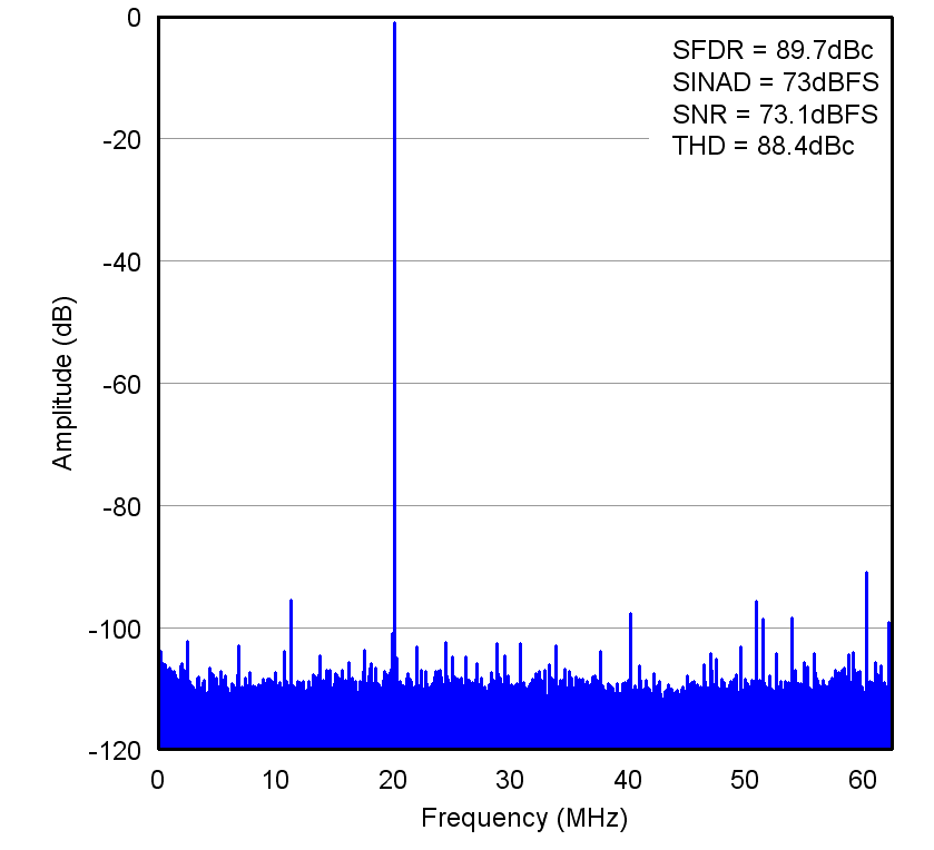 Figure 7-28 FFT
for 20-MHz Input Signal
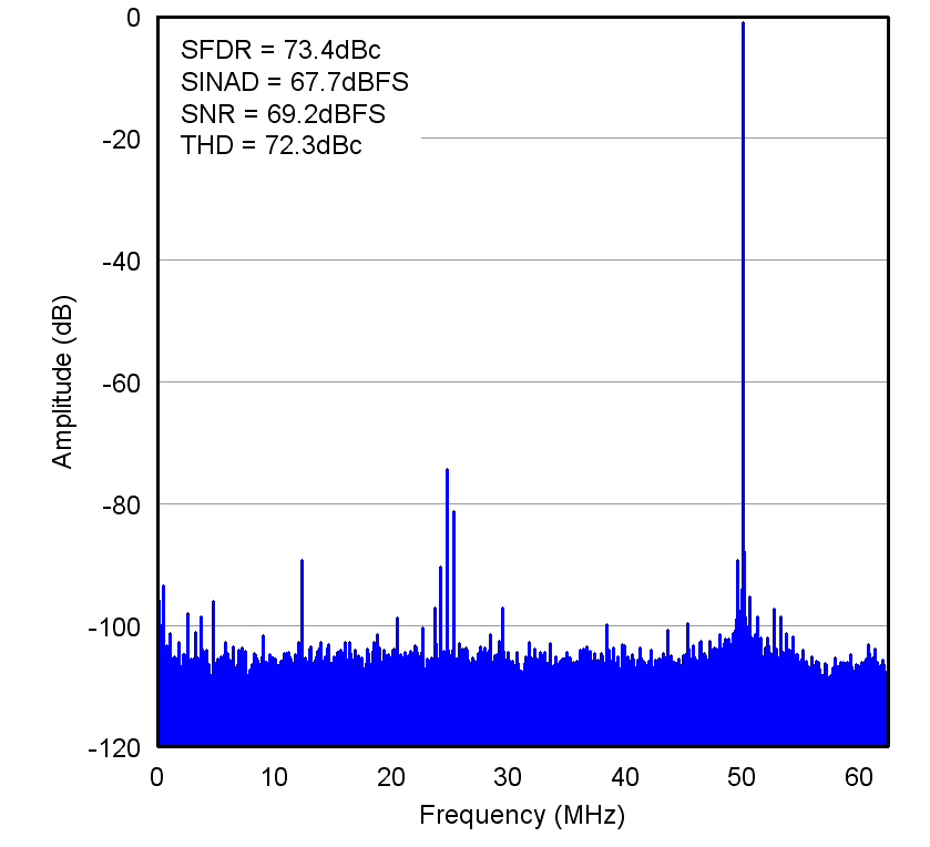 Figure 7-30 FFT
for 300-MHz Input Signal
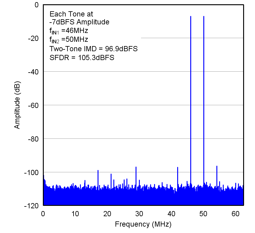 Figure 7-32 FFT
for Two-Tone Input Signal
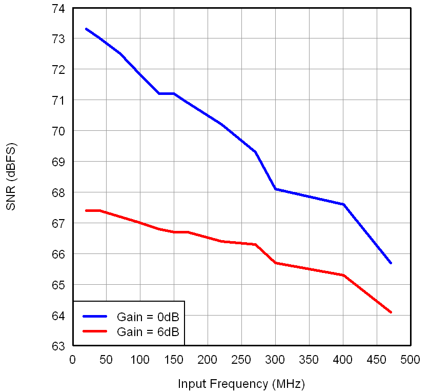 Figure 7-34 SNR
vs Input Frequency (CMOS)
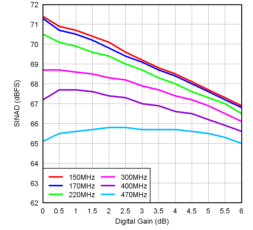 Figure 7-36 SINAD
vs Gain and Input Frequency
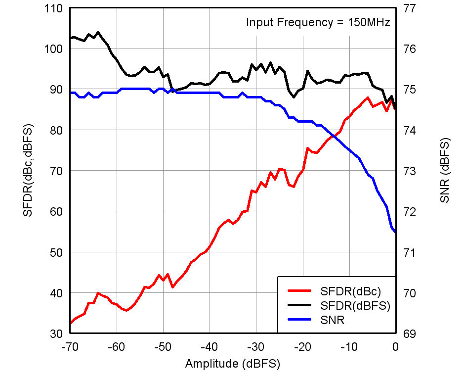 Figure 7-38 Performance vs Input Amplitude
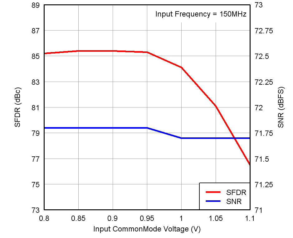 Figure 7-40 Performance vs Input Common-Mode Voltage
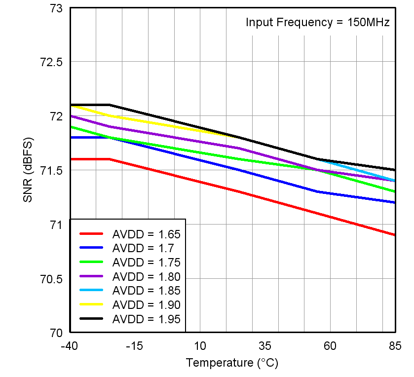 Figure 7-42 SNR
vs Temperature and AVDD Supply
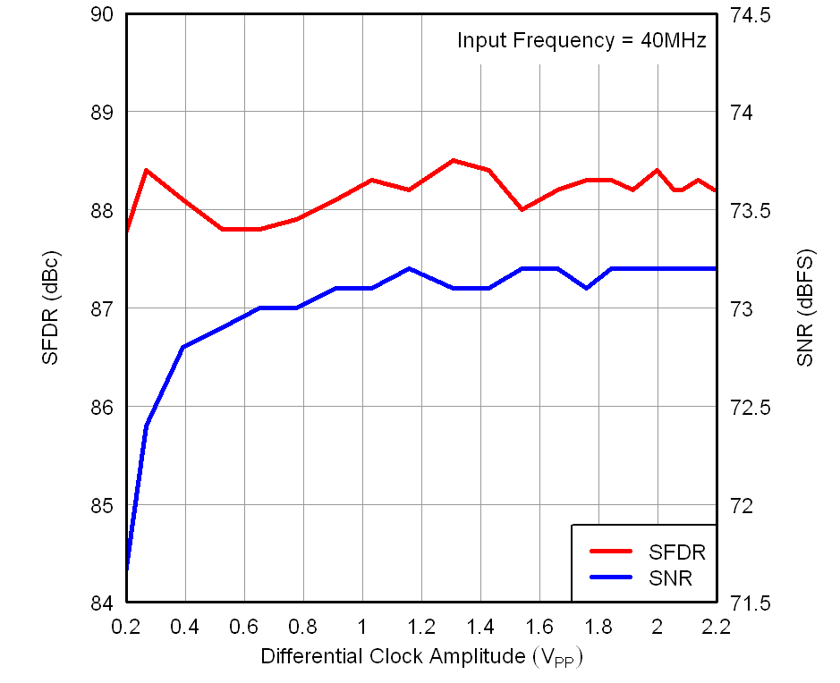 Figure 7-44 Performance vs Input Clock Amplitude
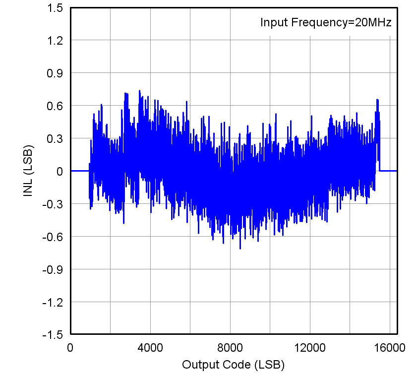 Figure 7-46 Integrated Nonlinearity
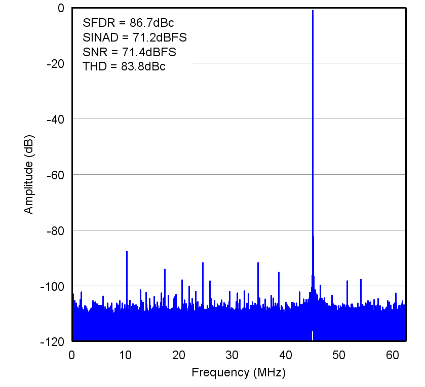 Figure 7-29 FFT
for 170-MHz Input Signal
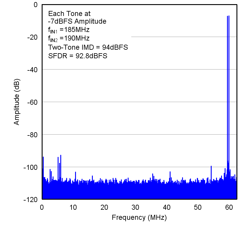 Figure 7-31 FFT
for Two-Tone Input Signal
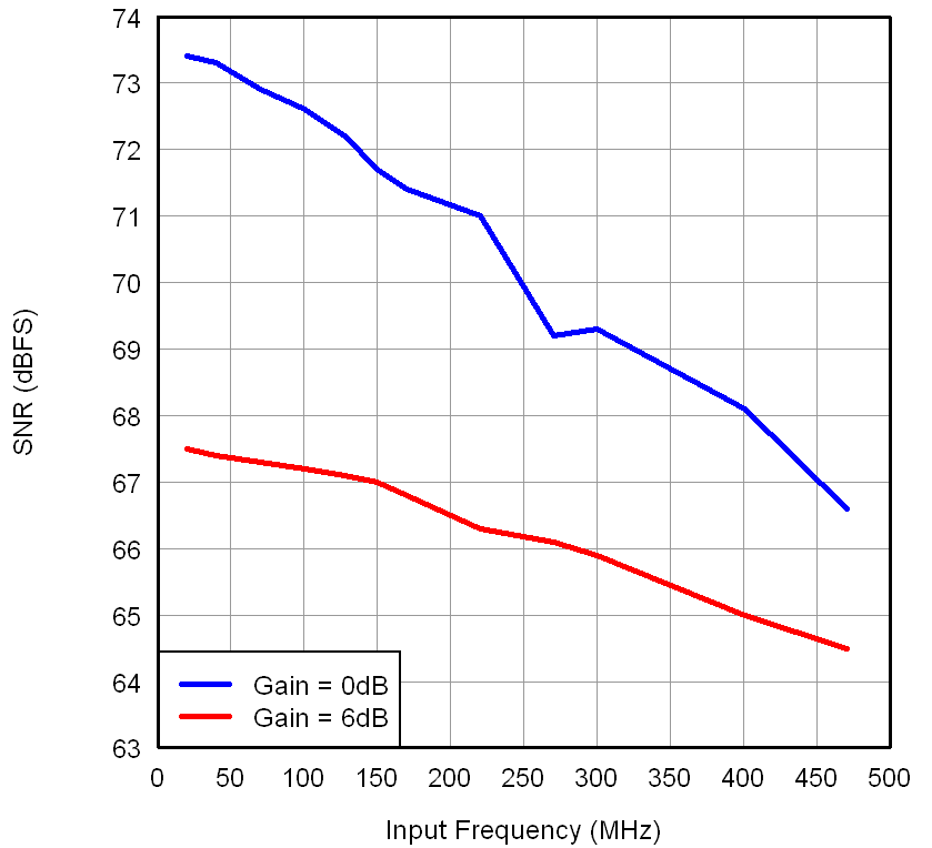 Figure 7-33 SNR
vs Input Frequency
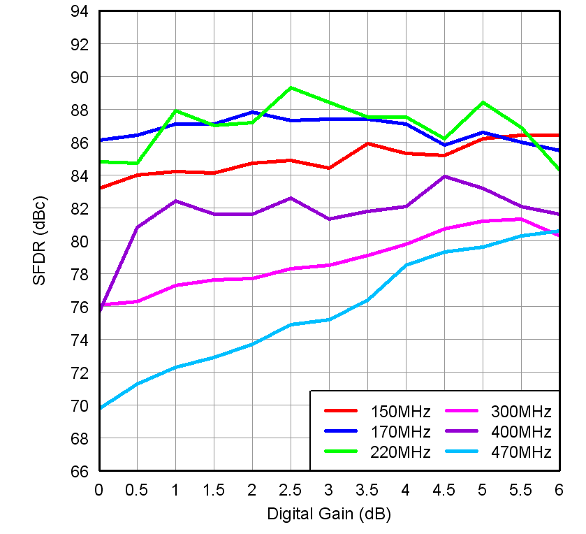 Figure 7-35 SFDR
vs Gain and Input Frequency
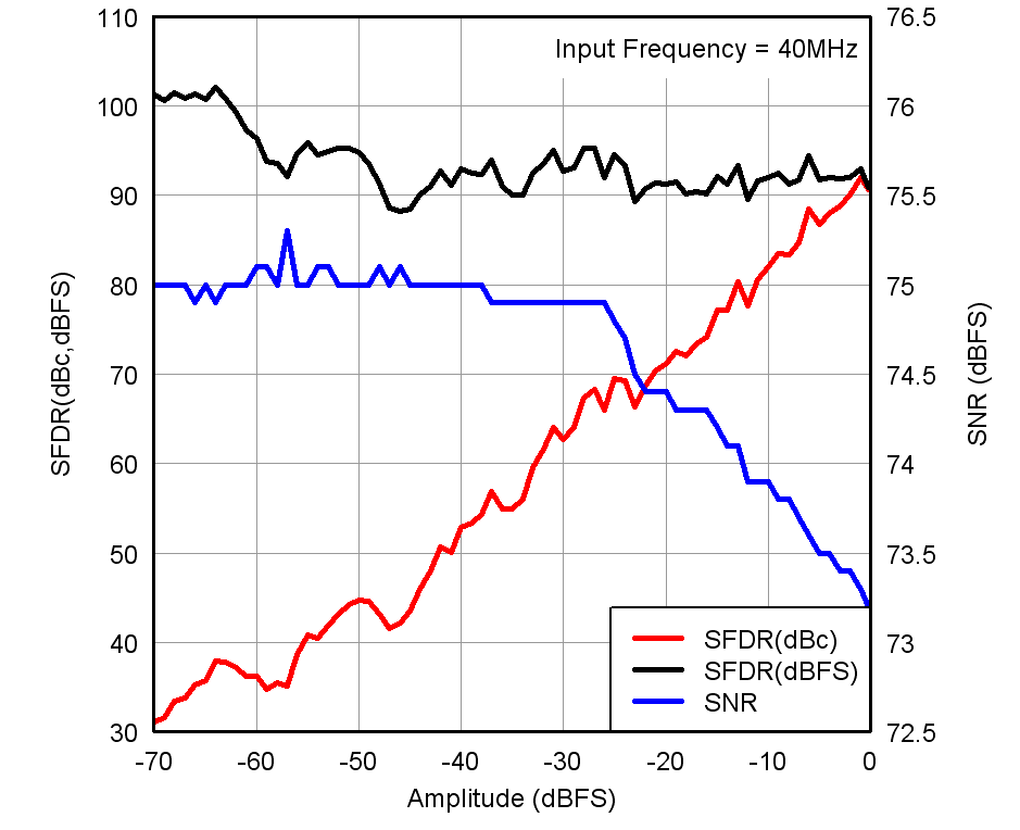 Figure 7-37 Performance vs Input Amplitude
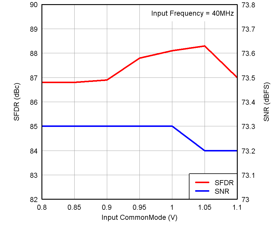 Figure 7-39 Performance vs Input Common-Mode Voltage
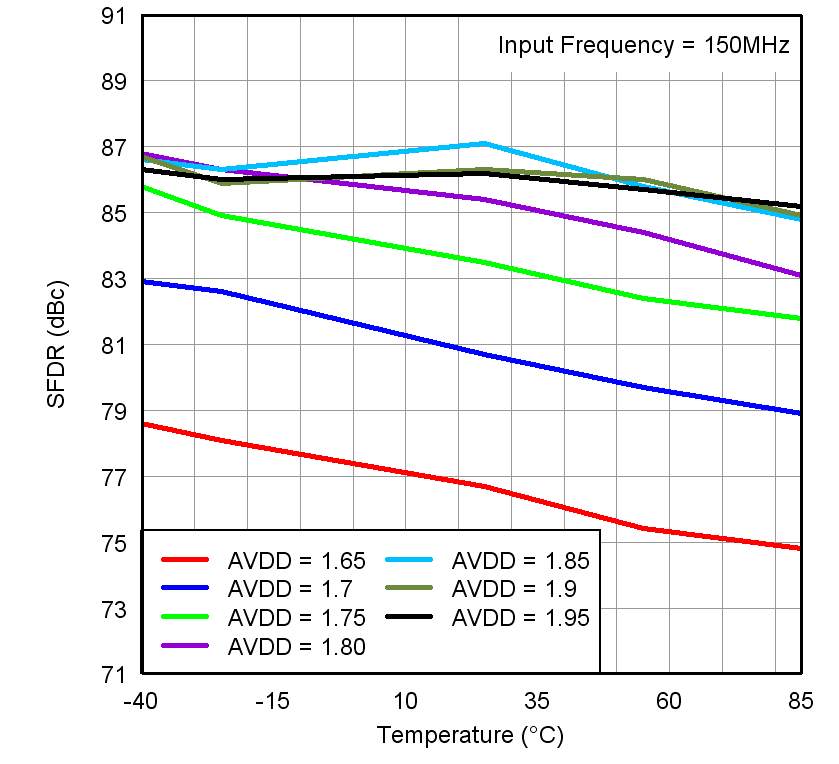 Figure 7-41 SFDR
vs Temperature and AVDD Supply
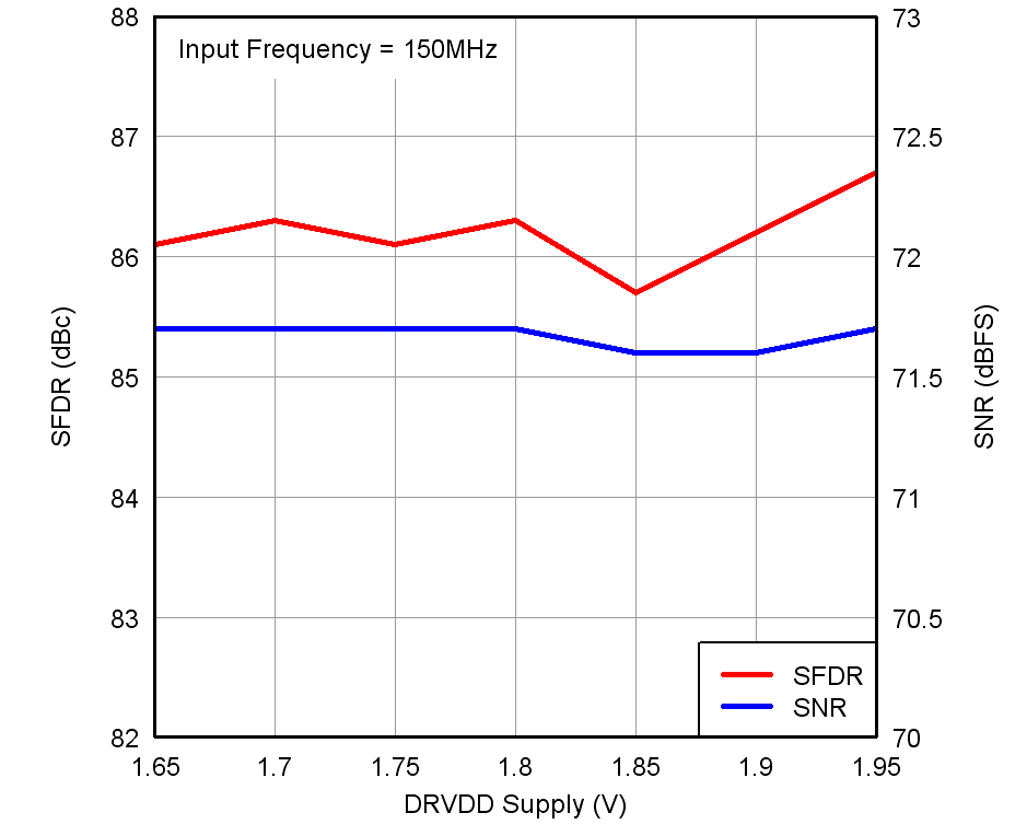 Figure 7-43 Performance vs DRVDD Supply Voltage
 Figure 7-45 Performance vs Input Clock Duty Cycle
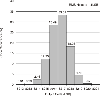 Figure 7-47 Output Noise Histogram (With Inputs Shorted to VCM)