ZHCSCA6B April 2014 – October 2020 ADS4245-EP
PRODUCTION DATA
- 1 特性
- 2 应用
- 3 说明
- 4 Revision History
- 5 Pin Configuration and Functions
-
6 Specifications
- 6.1 Absolute Maximum Ratings
- 6.2 ESD Ratings
- 6.3 Recommended Operating Conditions
- 6.4 Thermal Information
- 6.5 Electrical Characteristics:
- 6.6 Electrical Characteristics: General
- 6.7 Digital Characteristics
- 6.8 Timing Characteristics: LVDS And CMOS Modes
- 6.9 Typical Characteristics:
- 6.10 Typical Characteristics: General
- 6.11 Typical Characteristics: Contour
-
7 Detailed Description
- 7.1 Overview
- 7.2 Functional Block Diagram
- 7.3 Feature Description
- 7.4 Device Functional Modes
- 7.5 Serial Register Map
- 7.6 Description Of Serial Registers
- 8 Application and Implementation
- 9 Power Supply Recommendations
- 10Layout
- 11Device and Documentation Support
6.7 Digital Characteristics
At AVDD = 1.8V and DRVDD = 1.8V (unless otherwise noted). DC specifications refer to the condition where the digital outputs do not switch, but are permanently at a valid logic level '0' or '1'.
| PARAMETER | TEST CONDITIONS | MIN | TYP | MAX | UNIT | |
|---|---|---|---|---|---|---|
| DIGITAL INPUTS (RESET, SCLK, SDATA, SEN, CTRL1, CTRL2, CTRL3)(1) | ||||||
| High-level input voltage | All digital inputs support 1.8V and 3.3V CMOS logic levels | 1.3 | V | |||
| Low-level input voltage | 0.4 | V | ||||
| High-level input current | SDATA, SCLK(2) | VHIGH = 1.8V | 10 | µA | ||
| SEN(3) | VHIGH = 1.8V | 0 | µA | |||
| Low-level input current | SDATA, SCLK | VLOW = 0V | 0 | µA | ||
| SEN | VLOW = 0V | 10 | µA | |||
| DIGITAL OUTPUTS, CMOS INTERFACE (DA[13:0], DB[13:0], CLKOUT, SDOUT) | ||||||
| High-level output voltage | DRVDD – 0.1 | DRVDD | V | |||
| Low-level output voltage | 0 | 0.1 | V | |||
| Output capacitance (internal to device) | pF | |||||
| DIGITAL OUTPUTS, LVDS INTERFACE | ||||||
| High-level output differential voltage | VODH | With an external 100Ω termination | 220 | 350 | 490 | mV |
| Low-level output differential voltage | VODL | With an external 100Ω termination | –490 | –350 | –220 | mV |
| Output common-mode voltage | VOCM | 0.9 | 1.05 | 1.25 | V | |
(1) SCLK, SDATA, and SEN function as digital input terminals in serial configuration mode.
(2) SDATA, SCLK have internal 150kΩ pull-down resistor.
(3) SEN has an internal 150kΩ pull-up resistor to AVDD. Because the pull-up is weak, SEN can also be driven by 1.8V or 3.3V CMOS buffers.

With external 100Ω termination.
Figure 6-1 LVDS Output Voltage Levels
See datasheet for absolute maximum and minimum recommended operating conditions.
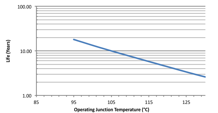
Silicon operating life design goal is 10 years at 105°C junction temperature (does not include package interconnect life).
Enhanced plastic product disclaimer applies.
Figure 6-2 ADS4245-EP Electromigration Fail Mode Chart