ZHCSCA6B April   2014  – October 2020 ADS4245-EP

PRODUCTION DATA  

  1. 特性
  2. 应用
  3. 说明
  4. Revision History
  5. Pin Configuration and Functions
  6. Specifications
    1. 6.1  Absolute Maximum Ratings
    2. 6.2  ESD Ratings
    3. 6.3  Recommended Operating Conditions
    4. 6.4  Thermal Information
    5. 6.5  Electrical Characteristics:
    6. 6.6  Electrical Characteristics: General
    7. 6.7  Digital Characteristics
    8. 6.8  Timing Characteristics: LVDS And CMOS Modes
    9. 6.9  Typical Characteristics:
    10. 6.10 Typical Characteristics: General
    11. 6.11 Typical Characteristics: Contour
  7. Detailed Description
    1. 7.1 Overview
    2. 7.2 Functional Block Diagram
    3. 7.3 Feature Description
    4. 7.4 Device Functional Modes
      1. 7.4.1 Digital Functions
      2. 7.4.2 Gain For SFDR/SNR Trade-Off
      3. 7.4.3 Offset Correction
      4. 7.4.4 Power-Down
        1. 7.4.4.1 Global Power-Down
        2. 7.4.4.2 Channel Standby
        3. 7.4.4.3 Input Clock Stop
      5. 7.4.5 Digital Output Information
        1. 7.4.5.1 Output Interface
        2. 7.4.5.2 DDR LVDS Outputs
        3. 7.4.5.3 LVDS Buffer
        4. 7.4.5.4 Parallel CMOS Interface
        5. 7.4.5.5 CMOS Interface Power Dissipation
        6. 7.4.5.6 Multiplexed Mode Of Operation
        7. 7.4.5.7 Output Data Format
      6. 7.4.6 Device Configuration
        1. 7.4.6.1 Parallel Configuration Only
        2. 7.4.6.2 Serial Interface Configuration Only
        3. 7.4.6.3 Using Both Serial Interface And Parallel Controls
        4. 7.4.6.4 Parallel Configuration Details
        5. 7.4.6.5 Serial Interface Details
          1. 7.4.6.5.1 Register Initialization
          2. 7.4.6.5.2 Serial Register Readout
    5. 7.5 Serial Register Map
    6. 7.6 Description Of Serial Registers
  8. Application and Implementation
    1. 8.1 Application Information
      1. 8.1.1 Clock Input
    2. 8.2 Typical Applications
      1. 8.2.1 Analog Input
        1. 8.2.1.1 Design Requirements for Drive Circuits
        2. 8.2.1.2 Detailed Design Procedure
        3. 8.2.1.3 Application Curves
  9. Power Supply Recommendations
  10. 10Layout
    1. 10.1 Layout Guidelines
      1. 10.1.1 Grounding
      2. 10.1.2 Supply Decoupling
      3. 10.1.3 Exposed Pad
      4. 10.1.4 Routing Analog Inputs
    2. 10.2 Layout Example
  11. 11Device and Documentation Support
    1. 11.1 Device Support
      1. 11.1.1 Device Support
        1. 11.1.1.1 Definition Of Specifications
    2. 11.2 Receiving Notification of Documentation Updates
    3. 11.3 Support Resources
    4. 11.4 Trademarks
    5. 11.5 Electrostatic Discharge Caution
    6. 11.6 Glossary

封装选项

机械数据 (封装 | 引脚)
散热焊盘机械数据 (封装 | 引脚)
订购信息

Multiplexed Mode Of Operation

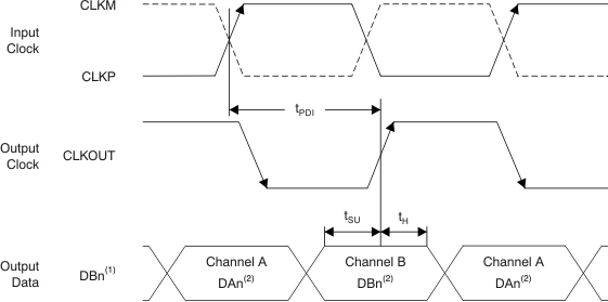
In this mode, the digital outputs of both channels are multiplexed and output on a single bus (DB[13:0] terminals), as shown in Figure 7-7. The channel A output terminals (DA[13:0]) are in 3-state. Because the output data rate on the DB bus is effectively doubled, this mode is recommended only for low sampling frequencies (less than 80MSPS). This mode can be enabled using the POWER-DOWN MODE register bits or using the CTRL[3:1] parallel terminals.
GUID-7A1D6864-A9E1-47B6-879C-D888A200BA94-low.gif
In multiplexed mode, both channels outputs come on the channel B output terminals.
Dn = bits D0, D1, D2, etc.
Figure 7-7 Multiplexed Mode Timing Diagram