ZHCS114E march 2011 – february 2023 ADS4222 , ADS4225 , ADS4226 , ADS4242 , ADS4245 , ADS4246
PRODUCTION DATA
- 1 特性
- 2 应用
- 3 说明
- 4 Revision History
- 5 说明(续)
- 6 Pin Configuration and Functions
-
7 Specifications
- 7.1 Absolute Maximum Ratings
- 7.2 ESD Ratings
- 7.3 Recommended Operating Conditions
- 7.4 Thermal Information
- 7.5 Electrical Characteristics: ADS4246, ADS4245, ADS4242
- 7.6 Electrical Characteristics: ADS4226, ADS4225, ADS4222
- 7.7 Electrical Characteristics: General
- 7.8 Digital Characteristics
- 7.9 Timing Requirements: LVDS and CMOS Modes #GUID-C6C0701B-A11B-492F-BD6B-B774F5FE4665/SLAS6895399
- 7.10 Serial Interface Timing Characteristics #GUID-3852E7CE-C5B6-42F5-A56A-70AB1B981302/SBAS5097810
- 7.11 Reset Timing (Only When Serial Interface Is Used)
- 7.12 Typical Characteristics
-
8 Detailed Description
- 8.1 Overview
- 8.2 Functional Block Diagrams
- 8.3 Feature Description
- 8.4 Device Functional Modes
- 8.5 Programming
- 8.6 Register Maps
- 9 Application and Implementation
- 10Device and Documentation Support
- 11Mechanical, Packaging, and Orderable Information
8.5.7.3 LVDS Buffer
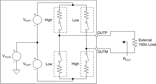
The equivalent circuit of each LVDS output buffer is shown in Figure 8-22. After reset, the buffer presents an output impedance of 100 Ω to match with the external 100-Ω termination.

The VDIFF voltage is nominally 350 mV, resulting in an output swing of ±350 mV with 100-Ω external termination. The VDIFF voltage is programmable using the LVDS SWING register bits from ±125 mV to ±570 mV.
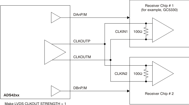
Additionally, a mode exists to double the strength of the LVDS buffer to support 50-Ω differential termination, as shown in Figure 8-23. This mode can be used when the output LVDS signal is routed to two separate receiver chips, each using a 100-Ω termination. The mode can be enabled using the LVDS DATA STRENGTH and LVDS CLKOUT STRENGTH register bits for data and output clock buffers, respectively.
The buffer output impedance behaves in the same way as a source-side series termination. By absorbing reflections from the receiver end, it helps to improve signal integrity.
 Figure 8-23 LVDS Buffer Differential Termination