ZHCSAK5C
December 2012 – December 2015
ADS42B49
PRODUCTION DATA.
1
特性
2
应用
3
说明
4
修订历史记录
5
Description (continued)
6
ADS424x and ADS422x Family Comparison
7
Pin Configuration and Functions
8
Specifications
8.1
Absolute Maximum Ratings
8.2
ESD Ratings
8.3
Recommended Operating Conditions
8.4
Thermal Information
8.5
Electrical Characteristics: ADS42B49 (250 MSPS)
8.6
Electrical Characteristics: General
8.7
Digital Characteristics
8.8
Timing Requirements: LVDS and CMOS Modes
8.9
Serial Interface Timing Characteristics
8.10
Reset Timing (Only When Serial Interface is Used)
8.11
LVDS Timings at Lower Sampling Frequencies
8.12
CMOS Timings at Lower Sampling Frequencies
8.13
Typical Characteristics
8.13.1
ADS42B49
8.13.2
Contour
9
Parameter Measurement Information
10
Detailed Description
10.1
Overview
10.2
Functional Block Diagram
10.3
Feature Description
10.3.1
Migrating from the ADS62P49 and ADS4249
10.3.2
Digital Functions
10.3.3
Gain for SFDR and SNR Trade-Off
10.3.4
Offset Correction
10.4
Device Functional Modes
10.4.1
Power-Down
10.4.1.1
Global Power-Down
10.4.1.2
Channel Standby
10.4.1.3
Input Clock Stop
10.4.2
Digital Output Information
10.4.2.1
Output Interface
10.4.2.2
DDR LVDS Outputs
10.4.2.3
LVDS Buffer
10.4.2.4
Parallel CMOS Interface
10.4.2.5
CMOS Interface Power Dissipation
10.4.2.6
Multiplexed Mode of Operation
10.4.2.7
Output Data Format
10.4.3
Parallel Configuration Details
10.5
Programming
10.5.1
Parallel Configuration Only
10.5.2
Serial Interface Configuration Only
10.5.3
Using Both Serial Interface and Parallel Controls
10.5.4
Serial Interface Details
10.5.4.1
Register Initialization
10.5.4.2
Serial Register Readout
10.6
Register Maps
10.6.1
Register Description
11
Application and Implementation
11.1
Application Information
11.1.1
Driving Circuit
11.1.1.1
Drive Circuit Requirements
11.1.2
Clock Input
11.2
Typical Application
11.2.1
Design Requirements
11.2.2
Detailed Design Procedure
11.2.2.1
Analog Input
11.2.2.2
Clock Driver
11.2.2.3
Digital Interface
11.2.3
Application Curves
12
Power Supply Recommendations
12.1
Using DC/DC Power Supplies
12.2
Power Supply Bypassing
13
Layout
13.1
Layout Guidelines
13.1.1
Grounding
13.1.2
Supply Decoupling
13.1.3
Exposed Pad
13.1.4
Routing Analog Inputs
13.2
Layout Example
14
器件和文档支持
14.1
器件支持
14.1.1
器件命名规则
14.2
文档支持
14.2.1
相关文档
14.3
社区资源
14.4
商标
14.5
静电放电警告
14.6
Glossary
15
机械、封装和可订购信息
封装选项
机械数据 (封装 | 引脚)
RGC|64
MPQF125F
散热焊盘机械数据 (封装 | 引脚)
RGC|64
QFND123N
订购信息
zhcsak5c_oa
zhcsak5c_pm
9 Parameter Measurement Information
1. With an external 100-Ω termination.
Figure 37. LVDS Output Voltage Levels
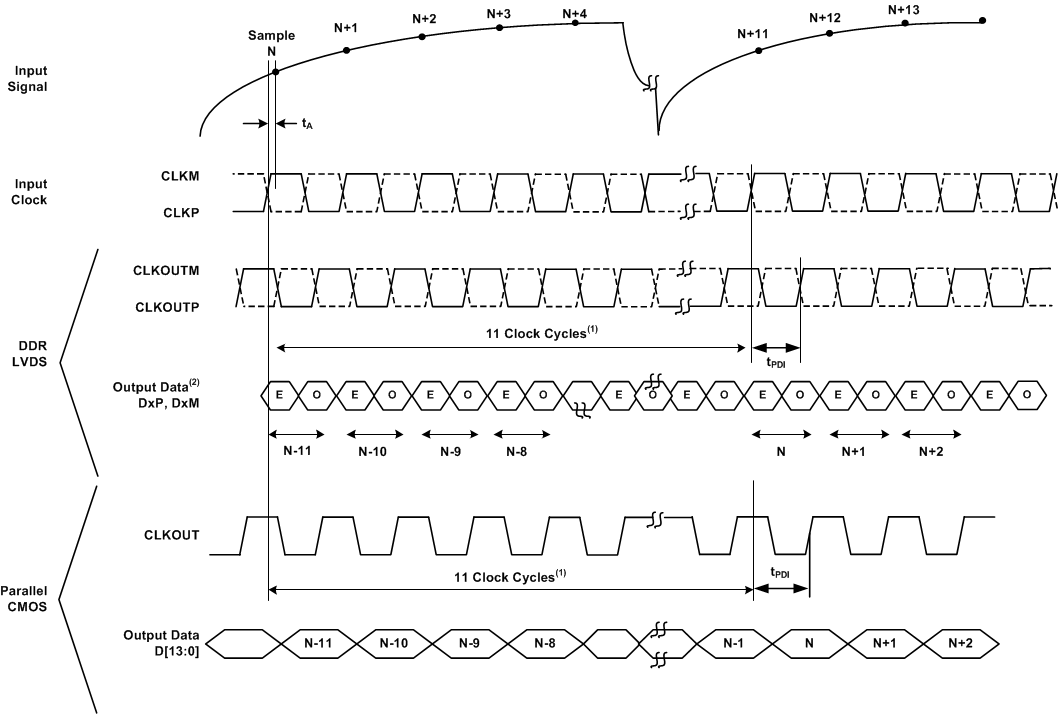
1. The ADC latency after reset is 11 clock cycles. Overall latency = ADC latency + t
PDI
.
2. E = even bits (D0, D2, D4, and so forth); O = odd bits (D1, D3, D5, and so forth).
Figure 38. Latency Timing Diagram
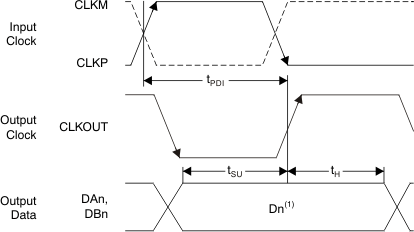
1. D
n
= bits D0, D1, D2, and so forth of channels A and B.
Figure 39. CMOS Interface Timing Diagram
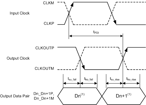
1. D
n
= D0, D2, D4, and so forth. D
n
+1 = D1, D3, D5, and so forth.
Figure 40. LVDS Interface Timing Diagram
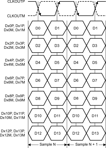
Figure 41. LVDS Bit Order
千亿体育app官网登录(中国)官方网站IOS/安卓通用版/手机APP
|
米乐app下载官网(中国)|ios|Android/通用版APP最新版
|
米乐|米乐·M6(中国大陆)官方网站
|
千亿体育登陆地址
|
华体会体育(中国)HTH·官方网站
|
千赢qy国际_全站最新版千赢qy国际V6.2.14安卓/IOS下载
|
18新利网v1.2.5|中国官方网站
|
bob电竞真人(中国官网)安卓/ios苹果/电脑版【1.97.95版下载】
|
千亿体育app官方下载(中国)官方网站IOS/安卓/手机APP下载安装
|