ZHCSBL9F October 2012 – May 2016 ADS42LB49 , ADS42LB69
PRODUCTION DATA.
- 1 特性
- 2 应用
- 3 说明
- 4 修订历史记录
- 5 Pin Configuration and Functions
-
6 Specifications
- 6.1 Absolute Maximum Ratings
- 6.2 ESD Ratings
- 6.3 Recommended Operating Conditions
- 6.4 Thermal Information
- 6.5 Electrical Characteristics: ADS42LB69 (16-Bit)
- 6.6 Electrical Characteristics: ADS42LB49 (14-Bit)
- 6.7 Electrical Characteristics: General
- 6.8 Digital Characteristics
- 6.9 Timing Requirements: General
- 6.10 Timing Requirements: DDR LVDS Mode
- 6.11 Timing Requirements: QDR LVDS Mode
- 6.12 Typical Characteristics: ADS42LB69
- 6.13 Typical Characteristics: ADS42LB49
- 6.14 Typical Characteristics: Common
- 6.15 Typical Characteristics: Contour
- 7 Parameter Measurement Information
-
8 Detailed Description
- 8.1 Overview
- 8.2 Functional Block Diagrams
- 8.3 Feature Description
- 8.4 Device Functional Modes
- 8.5 Programming
- 8.6
Register Maps
- 8.6.1
Description of Serial Interface Registers
- 8.6.1.1 Register 6 (offset = 06h) [reset = 80h]
- 8.6.1.2 Register 7 (offset = 07h) [reset = 00h]
- 8.6.1.3 Register 8 (offset = 08h) [reset = 00h]
- 8.6.1.4 Register B (offset = 0Bh) [reset = 00h]
- 8.6.1.5 Register C (offset = 0Ch) [reset = 00h]
- 8.6.1.6 Register D (offset = 0Dh) [reset = 6Ch]
- 8.6.1.7 Register F (offset = 0Fh) [reset = 00h]
- 8.6.1.8 Register 10 (offset = 10h) [reset = 00h]
- 8.6.1.9 Register 11 (offset = 11h) [reset = 00h]
- 8.6.1.10 Register 12 (offset = 12h) [reset = 00h]
- 8.6.1.11 Register 13 (offset = 13h) [reset = 00h]
- 8.6.1.12 Register 14 (offset = 14h) [reset = 00h]
- 8.6.1.13 Register 15 (offset = 15h) [reset = 00h]
- 8.6.1.14 Register 16 (offset = 16h) [reset = 00h]
- 8.6.1.15 Register 17 (offset = 17h) [reset = 00h]
- 8.6.1.16 Register 18 (offset = 18h) [reset = 00h]
- 8.6.1.17 Register 1F (offset = 1Fh) [reset = 7Fh]
- 8.6.1.18 Register 20 (offset = 20h) [reset = 00h]
- 8.6.1
Description of Serial Interface Registers
- 9 Application and Implementation
- 10Power Supply Recommendations
- 11Layout
- 12器件和文档支持
- 13机械、封装和可订购信息
8 Detailed Description
8.1 Overview
The ADS42LB69 and ADS42LB49 is a family of high linearity, buffered analog input, dual-channel ADCs with maximum sampling rates up to 250 MSPS employing either a quadruple data rate (QDR) or double data rate (DDR) LVDS interface. The conversion process is initiated by a rising edge of the external input clock and the analog input signal is sampled. The sampled signal is sequentially converted by a series of small resolution stages, with the outputs combined in a digital correction logic block. At every clock edge the sample propagates through the pipeline, resulting in a data latency of 14 clock cycles. The output is available in LVDS logic levels in SPI-programmable QDR or DDR options.
8.2 Functional Block Diagrams
 Figure 76. ADS42LB69 DDR LVDS
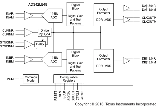 Figure 77. ADS42LB49 DDR LVDS
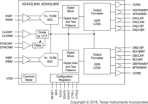 Figure 78. ADS42LB69, ADS42LB49 QDR LVDS
8.3 Feature Description
8.3.1 Digital Gain
The device includes gain settings that can be used to obtain improved SFDR performance (compared to no gain). Gain is programmable from –2 dB to 6 dB (in 0.5-dB steps). For each gain setting, the analog input full-scale range scales proportionally. Table 3 shows how full-scale input voltage changes when digital gain are programmed in 1-dB steps. Refer to Table 16 to set digital gain using a serial interface register.
SFDR improvement is achieved at the expense of SNR; for a 1-dB increase in digital gain, SNR degrades approximately between 0.5 dB and 1 dB (refer to Figure 15 and Figure 16). Therefore, gain can be used as a trade-off between SFDR and SNR. Note that the default gain after reset is 0 dB with a 2.0-VPP full-scale voltage.
Table 3. Full-Scale Range Across Gains
| DIGITAL GAIN | FULL-SCALE INPUT VOLTAGE |
|---|---|
| –2 dB | 2.5 VPP(1) |
| –1 dB | 2.2 VPP |
| 0 dB (default) | 2.0 VPP |
| 1 dB | 1.8 VPP |
| 2 dB | 1.6 VPP |
| 3 dB | 1.4 VPP |
| 4 dB | 1.25 VPP |
| 5 dB | 1.1 VPP |
| 6 dB | 1.0 VPP |
8.3.2 Input Clock Divider
The device is equipped with an internal divider on the clock input. This divider allows operation with a faster input clock, simplifying the system clock distribution design. The clock divider can be bypassed (divide-by-1) for operation with a 250-MHz clock. The divide-by-2 option supports a maximum 500-MHz input clock and the divide-by-4 option supports a maximum 1-GHz input clock frequency.
8.3.3 Overrange Indication
The device provides two different overrange indications: normal OVR and fast OVR. Normal OVR (default) is triggered if the final 16-bit data output exceeds the maximum code value. Normal OVR latency is the same as the output data (that is, 14 clock cycles). Fast OVR is triggered if the input voltage exceeds the programmable overrange threshold and is presented after a latency of only nine clock cycles, thus enabling a quicker reaction to an overrange event.
8.3.3.1 OVR in a QDR Pinout
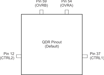
In a QDR interface, the overrange indication is output on the OVRA and OVRB pins (pin 54 and 59) in 1.8-V CMOS logic levels. The same overrange indication can also be made available on the bidirectional CTRL1, CTRL2 pins by using the PDN/OVR FOR CTRL PINS register bit, as described in Figure 79. Using the FAST OVR EN register bit, the fast OVR indication can be presented on these pins instead of normal OVR.
NOINDENT:
NOTE: By default, normal OVR is output on the OVRA and OVRB pins. Using the FAST OVR EN register bit, fast OVR can be presented on these pins instead.NOINDENT:
NOTE: When the PDN/OVR FOR CTRL PINS register bit is set, the CTRL1 and CTRL2 pins function as output pins and carry the same information as the OVRA and OVRB pins (respectively) in 1.8-V CMOS logic levels.8.3.3.2 OVR in a DDR Pinout
In the DDR interface, there are no dedicated pins to provide overrange indication. However, by choosing the appropriate register bits, OVR can be transferred on the LSB of 16-bit output data as well as on the bidirectional CTRL1 and CTRL2 pins, as shown in Figure 80.
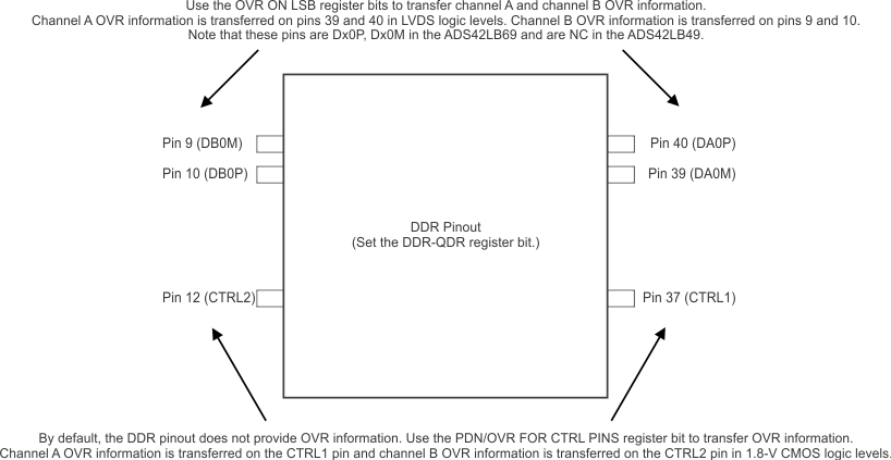 Figure 80. OVR in a DDR Pinout
The FAST OVR EN register bit can be used to transfer fast OVR indication on the CTRL1 and CTRL2 pins instead of normal OVR. The OVR ON LSB register bits can be used to transfer fast OVR indication on the LSB bits (Dx0P, Dx0M), as described in Table 4.
Table 4. Fast OVR Transfer
| OVR ON LSB BIT SETTINGS | PIN STATE FOR PINS 9, 10 AND 39, 40 |
|---|---|
| 00 | D0 and D1 are output in the ADS42LB69, NC for the ADS42LB49 |
| 01 | Fast OVR in LVDS logic level |
| 10 | Normal OVR in LVDS logic level |
| 11 | D0 and D1 are output in the ADS42LB69, NC for the ADS42LB49 |
Table 5 summarizes the availability of OVR information on different pins in the QDR and DDR interfaces and the required register settings.
Table 5. OVR Information Availability
| INTERFACE | SETTINGS | OVR INFORMATION AVAILABILITY | ||
|---|---|---|---|---|
| PINS 9, 10 AND 39, 40 (LVDS Logic Levels) | PINS 12 AND 37 (CMOS Logic Levels) |
PINS 54 AND 59 (CMOS Logic Levels) |
||
| QDR | Default | Not applicable | No | Yes |
| Use the PDN/OVR FOR CTRL PINS register bits | Not applicable | Yes | Yes | |
| DDR | Default | No | No | Not applicable |
| Use the OVR ON LSB register bits | Yes | No | Not applicable | |
| Use the PDN/OVR FOR CTRL PINS register bits | No | Yes | Not applicable | |
| Use the OVR ON LSB and PDN/OVR FOR CTRL PINS register bits | Yes | Yes | Not applicable | |
8.3.3.3 Programming Threshold for Fast OVR
The input voltage level at which the overload is detected is referred to as the threshold and is programmable using the FAST OVR THRESHOLD bits. Fast OVR is triggered nine output clock cycles after the overload condition occurs. The threshold voltage amplitude at which fast OVR is triggered is Equation 1:
When digital gain is programmed (for gain values > 0 dB ), the threshold voltage amplitude is Equation 2:
8.3.4 LVDS Buffer
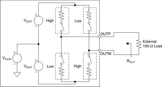
The equivalent circuit of each LVDS output buffer is shown in Figure 81. After reset, the buffer presents an output impedance of 100 Ω to match with the external 100-Ω termination.
NOINDENT:
NOTE: Default swing across 100-Ω load is ±350 mV. Use the LVDS SWING bits to change the swing.The VDIFF voltage is nominally 350 mV, resulting in an output swing of ±350 mV with 100-Ω external termination. The VDIFF voltage is programmable using the LVDS SWING register bits from ±125 mV to ±570 mV.
Additionally, a mode exists to double the strength of the LVDS buffer to support 50-Ω differential termination, as shown in Figure 82. This mode can be used when the output LVDS signal is routed to two separate receiver chips, each using a 100-Ω termination. The mode can be enabled for LVDS output data (and for the frame clock in the QDR interface) buffers by setting the LVDS DATA STRENGTH register bit. For LVDS output clock buffers (applicable for both DDR and QDR interfaces), set both the LVDS CLKOUT STRENGTH EN and LVDS CLKOUT STRENGTH register bits to '1'.
The buffer output impedance behaves in the same way as a source-side series termination. Absorbing reflections from the receiver end helps improve signal integrity.
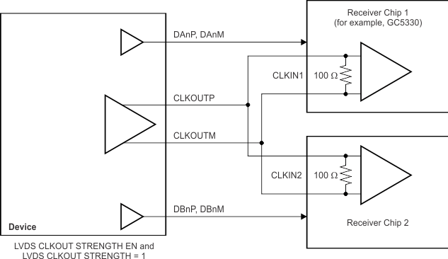 Figure 82. LVDS Buffer Differential Termination
8.3.5 Output Data Format
Two output data formats are supported: twos complement and offset binary. The format can be selected using the DATA FORMAT serial interface register bit.
In the event of an input voltage overdrive, the digital outputs go to the appropriate full-scale level. For a positive overdrive, the output code is 3FFFh for the ADS42LB49 and ADS42LB69 in offset binary output format; the output code is 1FFFh for the ADS42LB49 and ADS42LB69 in twos complement output format. For a negative input overdrive, the output code is 0000h in offset binary output format and 2000h for the ADS42LB49 and ADS42LB69 in twos complement output format.
8.4 Device Functional Modes
8.4.1 Digital Output Information
The ADS42LB49 and ADS42LB69 provides 14- and 16-bit digital data for each channel and output clock synchronized with the data.
8.4.1.1 Output Interface
Digital outputs are available in quadruple data rate (QDR) LVDS, and double data rate (DDR) LVDS formats, selectable by the DDR – QDR serial register bit.
8.4.1.2 DDR LVDS Outputs
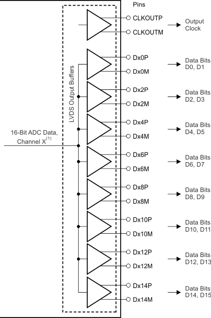
In this mode, the data bits and clock are output using low-voltage differential signal (LVDS) levels. Two data bits are multiplexed and output on each LVDS differential pair, as shown in Figure 83.
NOINDENT:
X = A or B (for channel A or channel B).Even data bits (D0, D2, D4, and so forth) are output at the CLKOUTP rising edge and the odd data bits (D1, D3, D5, and so forth) are output at the CLKOUTP falling edge. Both the CLKOUTP rising and falling edges must be used to capture all the data bits, as shown in Figure 84.
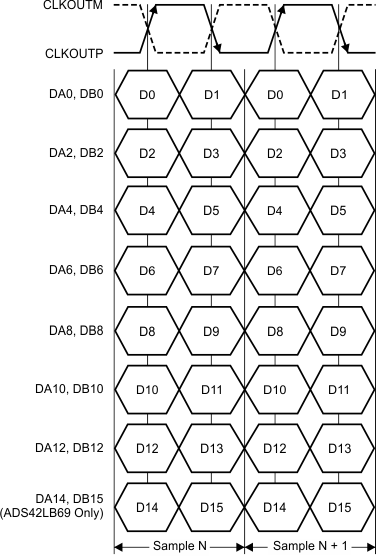 Figure 84. DDR LVDS Interface Timing
8.4.1.3 QDR LVDS Outputs
The data bits and output clocks are output using low-voltage differential signal (LVDS) levels. Four data bits are multiplexed and output on each LVDS differential data pair and are accompanied by a bit clock and a frame clock for each channel, as shown in Figure 85.
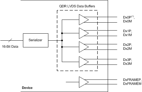
NOINDENT:
X = channels A and B.Figure 86 shows the QDR interface bit order for the ADS42LB69 and Figure 87 shows the QDR interface bit order for the ADS42LB49.
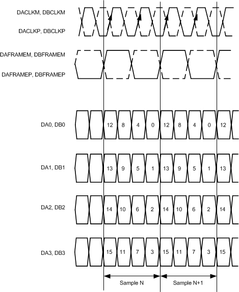 |
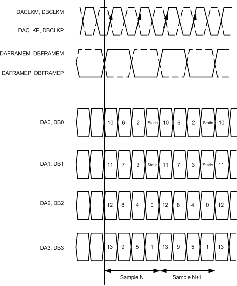 |
| Figure 86. QDR LVDS Interface Timing: ADS42LB69 | Figure 87. QDR LVDS Interface Timing: ADS42LB49 |
8.5 Programming
8.5.1 Device Configuration
The ADS42LB49 and ADS42LB69 can be configured using a serial programming interface, as described in this section. In addition, the device has two bidirectional parallel pins (CTRL1 and CTRL2). By default, these pins act as input pins and control the power-down modes, as described in Table 6 and Table 7. These pins can be programmed as output pins that deliver overrange information by setting the PDN/OVR_FOR_CTRL_PINS register bit.
Table 6. PDN/OVR_FOR_CTRL_PINS Bit (Set to '0')
| CTRL2 | CTRL1 | PIN DIRECTION | FUNCTION |
|---|---|---|---|
| Low | Low | Input | Default operation |
| Low | High | Input | Channel A power-down |
| High | Low | Input | Channel B powers down in QDR mode. Do not use in DDR mode. |
| High | High | Input | Channels A and B power-down |
Table 7. PDN/OVR_FOR_CTRL_PINS Bit (Set to '1')
| CTRL2 | CTRL1 | PIN DIRECTION |
|---|---|---|
| Carries OVR for channel B | Carries OVR for channel A | Output |
8.5.2 Details of Serial Interface
The ADC has a set of internal registers that can be accessed by the serial interface formed by the SEN (serial interface enable), SCLK (serial interface clock), SDATA (serial interface data) and SDOUT (serial interface data output) pins. Serial shift of bits into the device is enabled when SEN is low. Serial data SDATA are latched at every SCLK rising edge when SEN is active (low). The serial data are loaded into the register at every 16th SCLK rising edge when SEN is low. When the word length exceeds a multiple of 16 bits, the excess bits are ignored. Data can be loaded in multiples of 16-bit words within a single active SEN pulse. The interface can work with SCLK frequencies from 20 MHz down to very low speeds (of a few hertz) and also with non-50% SCLK duty cycle.
8.5.2.1 Register Initialization
After power-up, the internal registers must be initialized to their default values through a hardware reset by applying a high pulse on the RESET pin (of durations greater than 10 ns); see Figure 88 and Table 8. If required, serial interface registers can later be cleared during operation by:
- Either through a hardware reset or
- By applying a software reset. When using the serial interface, set the RESET bit (D0 in register address 08h) high. This setting initializes the internal registers to the default values and then self-resets the RESET bit low. In this case, the RESET pin is kept low.
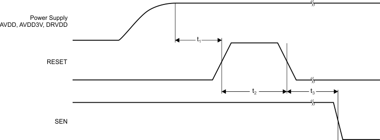
NOINDENT:
NOTE: After power-up, the internal registers must be initialized to their default values through a hardware reset by applying a high pulse on the RESET pin.Table 8. Reset Timing(1)
| TEST CONDITIONS | MIN | TYP | MAX | UNIT | ||
|---|---|---|---|---|---|---|
| t1 | Power-on delay | Delay from AVDD and DRVDD power-up to active RESET pulse | 1 | ms | ||
| t2 | Reset pulse width | Active RESET signal pulse width | 10 | ns | ||
| 1 | µs | |||||
| t3 | Register write delay | Delay from RESET disable to SEN active | 100 | ns | ||
8.5.2.2 Serial Register Write
The internal register of the ADS42LB49 and ADS42LB69 can be programmed following these steps:
- Drive SEN pin low
- Set the R/W bit to ‘0’ (bit A7 of the 8 bit address)
- Set bit A6 in the address field to ‘0’
- Initiate a serial interface cycle specifying the address of the register (A5 to A0) whose content must be written
- Write 8 bit data which is latched in on the rising edge of SCLK.
Figure 89 and Table 9 illustrate these steps.
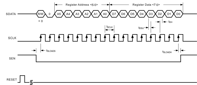 Figure 89. Serial Register Write Timing Diagram
Table 9. Serial Interface Timing (Only when Serial Interface is Used)(1)
| MIN | TYP | MAX | UNIT | ||
|---|---|---|---|---|---|
| fSCLK | SCLK frequency (equal to 1 / tSCLK) | > dc | 20 | MHz | |
| tSLOADS | SEN to SCLK setup time | 25 | ns | ||
| tSLOADH | SCLK to SEN hold time | 25 | ns | ||
| tDSU | SDIO setup time | 25 | ns | ||
| tDH | SDIO hold time | 25 | ns | ||
8.5.2.3 Serial Register Readout
The device includes a mode where the contents of the internal registers can be read back using the SDOUT pin. This read-back mode may be useful as a diagnostic check to verify the serial interface communication between the external controller and the ADC.
- Drive SEN pin low
- Set the R/W bit (A7) to '1'. This setting disables any further writes to the registers
- Set bit A6 in the address field to 0.
- Initiate a serial interface cycle specifying the address of the register (A5 to A0) whose content has to be read.
- The device outputs the contents (D7 to D0) of the selected register on the SDOUT pin.
- The external controller can latch the contents at the SCLK falling edge.
- To enable register writes, reset the R/W register bit to '0'.
Figure 90 illustrates these steps. When READOUT is disabled, the SDOUT pin is in a high-impedance mode. If serial readout is not used, the SDOUT pin must float.
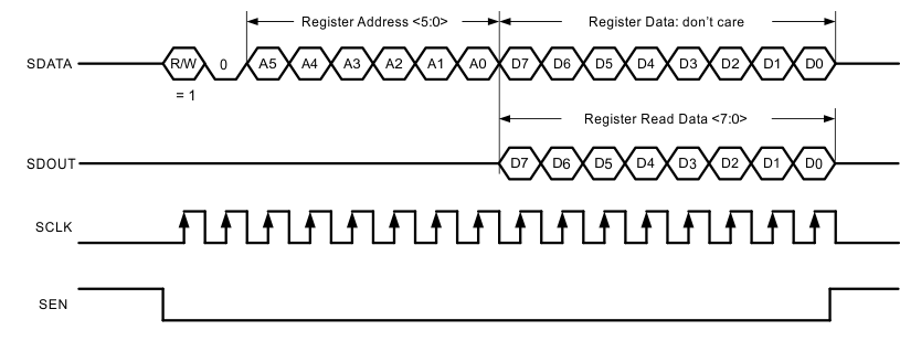 Figure 90. Serial Register Readout Timing Diagram
8.6 Register Maps
The serial interface registers are summarized in Table 10.
Table 10. Summary of Serial Interface Registers
Table 11. High-Frequency Modes Summary
| REGISTER ADDRESS | VALUE | DESCRIPTION |
|---|---|---|
| 0Dh | 90h | Enable high-frequency modes for input frequencies greater than 250 MHz. |
| 0Eh | 90h | Enable high-frequency modes for input frequencies greater than 250 MHz. |
8.6.1 Description of Serial Interface Registers
8.6.1.1 Register 6 (offset = 06h) [reset = 80h]
| D7 | D6 | D5 | D4 | D3 | D2 | D1 | D0 |
| 1 | 0 | 0 | 0 | 0 | 0 | CLK DIV | |
| W-1h | W-0h | W-0h | W-0h | W-0h | W-0h | R/W-0h | |
| LEGEND: R/W = Read/Write; W = Write only; -n = value after reset |
Table 12. (For example, CONTROL_REVISION Register) Field Descriptions
| Bit | Field | Type | Reset | Description |
|---|---|---|---|---|
| D7 | 1 | W | 1h | Always write '1' |
| D[6:2] | 0 | W | 0h | Always write '0' |
| D[1:0] | CLK DIV | R/W | 0h | Internal clock divider for input sample clock 00 : Divide-by-1 (clock divider bypassed) 01 : Divide-by-2 10 : Divide-by-1 11 : Divide-by-4 |
8.6.1.2 Register 7 (offset = 07h) [reset = 00h]
| D7 | D6 | D5 | D4 | D3 | D2 | D1 | D0 |
| 0 | 0 | 0 | 0 | 0 | SYNCIN DELAY | ||
| W-0h | W-0h | W-0h | W-0h | W-0h | R/W-0h | ||
| LEGEND: R/W = Read/Write; W = Write only; -n = value after reset |
Table 13. Register 7 Field Descriptions
| Bit | Field | Type | Reset | Description |
|---|---|---|---|---|
| D[7:3] | 0 | W | 0h | Always write '0' |
| D[2:0] | SYNCIN DELAY | R/W | 0h | Controls the delay of the SYNCIN input with respect to the input clock. Typical values for the expected delay of different settings are: 000 : 0-ps delay 001 : 60-ps delay 010 : 120-ps delay 011 : 180-ps delay 100 : 240-ps delay 101 : 300-ps delay 110 : 360-ps delay 111 : 420-ps delay |
8.6.1.3 Register 8 (offset = 08h) [reset = 00h]
| D7 | D6 | D5 | D4 | D3 | D2 | D1 | D0 |
| PDN CHA | PDN CHB | STDBY | DATA FORMAT | DIS CTRL PINS | TEST PAT ALIGN | 0 | RESET |
| R/W-0h | R/W-0h | R/W-0h | R/W-0h | R/W-0h | R/W-0h | W-0h | R/W-0h |
| LEGEND: R/W = Read/Write; W = Write only; -n = value after reset |
Table 14. Register 8 Field Descriptions
| Bit | Field | Type | Reset | Description |
|---|---|---|---|---|
| D[7:6] | PDN CHA, PDN CHB | R/W | 0h | Power-down channels A and B. Effective only when bit DIS CTRL PINS is set to '1'. 00 : Normal operation 01 : Channel B powers down. Use only if the QDR interface is selected. Do not use in the DDR interface. 10 : Channel A powers down. Functions in both QDR and DDR interfaces. 11 : Both channels power down. Functions in both QDR and DDR interfaces. |
| D5 | STDBY | R/W | 0h | Dual ADC is placed into standby mode 0 : Normal operation 1 : Power down |
| D4 | DATA FORMAT | R/W | 0h | Digital output data format 0 : Twos complement 1 : Offset binary |
| D3 | DIS CTRL PINS | R/W | 0h | Disables power-down control from the CTRL1, CTRL2 pins. This bit also functions as an enable bit for the INV CLK OUT CHA, INV CLK OUT CHB, and DDR OUTPUT TIMING bits. 0 : CTRL1 and CTRL2 pins control power-down options for channels A and B 1 : The PDN CHA and PDN CHB register bits determine power-down options for channels A and B. The INV CLK OUT CHA, INV CLK OUT CHB, and DDR OUTPUT TIMING register bits become effective. |
| D2 | TEST PAT ALIGN | R/W | 0h | Aligns test patterns of two channels 0 : Test patterns for channel A and channel B are free running 1 : Test patterns for both channels are synchronized |
| D1 | 0 | W | 0h | Always write '0' |
| D0 | RESET | R/W | 0h | Software reset applied This bit resets all internal registers to the default values and self-clears to ‘0’ |
8.6.1.4 Register B (offset = 0Bh) [reset = 00h]
| D7 | D6 | D5 | D4 | D3 | D2 | D1 | D0 |
| CHA GAIN | CHA GAIN EN | 0 | FLIP DATA | ||||
| R/W-0h | R/W-0h | W-0h | R/W-0h | ||||
| LEGEND: R/W = Read/Write; W = Write only; -n = value after reset |
Table 15. Register B Field Descriptions
| Bit | Field | Type | Reset | Description |
|---|---|---|---|---|
| D[7:3] | CHA GAIN | R/W | 0h | Digital gain for channel A. Effective when the CHA GAIN EN register bit is set to '1'. Bit descriptions are listed in Table 16. |
| D2 | CHA GAIN EN | R/W | 0h | Digital gain enable bit for channel A 0 : Digital gain disabled 1 : Digital gain enabled |
| D1 | 0 | W | 0h | Always write '0' |
| D0 | FLIP DATA | R/W | 0h | Flips bit order on the LVDS output bus (LSB versus MSB) 0 : Normal operation 1 : Output bus flipped. In the ADS42LB69, output data bit D0 becomes D15, D1 becomes D14, and so forth. In the ADS42LB49, output data bit D0 becomes D13, D1 becomes D12, and so forth. |
Table 16. Digital Gain for Channel A
| DIGITAL GAIN FOR CHANNEL A | DIGITAL GAIN (dB) | MAX INPUT VOLTAGE (VPP) | DIGITAL GAIN FOR CHANNEL A | DIGITAL GAIN (dB) | MAX INPUT VOLTAGE (VPP) | |
|---|---|---|---|---|---|---|
| 00000 | 0 | 2.0 | 01010 | 1.5 | 1.7 | |
| 00001 | Do not use | — | 01011 | 2 | 1.6 | |
| 00010 | Do not use | — | 01100 | 2.5 | 1.5 | |
| 00011 | –2.0 | 2.5 | 01101 | 3 | 1.4 | |
| 00100 | –1.5 | 2.4 | 01110 | 3.5 | 1.3 | |
| 00101 | –1.0 | 2.2 | 01111 | 4 | 1.25 | |
| 00110 | –0.5 | 2.1 | 10000 | 4.5 | 1.2 | |
| 00111 | 0 | 2.0 | 10001 | 5 | 1.1 | |
| 01000 | 0.5 | 1.9 | 10010 | 5.5 | 1.05 | |
| 01001 | 1 | 1.8 | 10011 | 6 | 1.0 |
8.6.1.5 Register C (offset = 0Ch) [reset = 00h]
| D7 | D6 | D5 | D4 | D3 | D2 | D1 | D0 |
| CHB GAIN | CHB GAIN EN | OVR ON LSB | |||||
| R/W-0h | R/W-0h | R/W-0h | |||||
| LEGEND: R/W = Read/Write; -n = value after reset |
Table 17. Register C Field Descriptions
| Bit | Field | Type | Reset | Description |
|---|---|---|---|---|
| D[7:3] | CHB GAIN | R/W | 0h | Digital gain for channel B. Effective when the CHB GAIN EN register bit is set to '1'. Bit descriptions are listed in Table 18. |
| D2 | CHB GAIN EN | R/W | 0h | Digital gain enable bit for channel B 0 : Digital gain disabled 1 : Digital gain disabled |
| D[1:0] | OVR ON LSB | R/W | 0h | Functions only with the DDR interface option. Replaces the LSB pair of 16-bit data (D1, D0) with OVR information. See the Overrange Indication section. 00 : D1 and D0 are output in the ADS42LB69, NC for the ADS42LB49 01 : Fast OVR in LVDS logic level 10 : Normal OVR in LVDS logic level 11 : D1 and D0 are output in the ADS42LB69, NC for the ADS42LB49 |
Table 18. Digital Gain for Channel B
| DIGITAL GAIN FOR CHANNEL B | DIGITAL GAIN (dB) | MAX INPUT VOLTAGE (VPP) | DIGITAL GAIN FOR CHANNEL B | DIGITAL GAIN (dB) | MAX INPUT VOLTAGE (VPP) | |
|---|---|---|---|---|---|---|
| 00000 | 0 | 2.0 | 01010 | 1.5 | 1.7 | |
| 00001 | Do not use | — | 01011 | 2 | 1.6 | |
| 00010 | Do not use | — | 01100 | 2.5 | 1.5 | |
| 00011 | –2.0 | 2.5 | 01101 | 3 | 1.4 | |
| 00100 | –1.5 | 2.4 | 01110 | 3.5 | 1.3 | |
| 00101 | –1.0 | 2.2 | 01111 | 4 | 1.25 | |
| 00110 | –0.5 | 2.1 | 10000 | 4.5 | 1.2 | |
| 00111 | 0 | 2.0 | 10001 | 5 | 1.1 | |
| 01000 | 0.5 | 1.9 | 10010 | 5.5 | 1.05 | |
| 01001 | 1 | 1.8 | 10011 | 6 | 1.0 |
8.6.1.6 Register D (offset = 0Dh) [reset = 6Ch]
| D7 | D6 | D5 | D4 | D3 | D2 | D1 | D0 |
| 0 | 1 | 1 | 0 | 1 | 1 | 0 | FAST OVR ON PIN |
| W-0h | W-1h | W-1h | W-0h | W-1h | W-1h | W-0h | R/W-0h |
| LEGEND: R/W = Read/Write; W = Write only; -n = value after reset |
Table 19. Register D Field Descriptions
| Bit | Field | Type | Reset | Description |
|---|---|---|---|---|
| D7 | 0 | W | 0h | Always write '0' |
| D[6:5] | 1 | W | 1h | Always write '1' |
| D4 | 0 | W | 0h | Always write '0' |
| D[3:2] | 1 | W | 1h | Always write '1' |
| D1 | 0 | W | 0h | Always write '0' |
| D0 | FAST OVR ON PIN | R/W | 0h | Determines whether normal OVR or fast OVR information is brought on the OVRx, CTRL1, and CTRL2 pins. See the Overrange Indication section. 0 : Normal OVR available on the OVRx, CTRL1, and CTRL2 pins 1 : Fast OVR available on the OVRx, CTRL1, and CTRL2 pins |
8.6.1.7 Register F (offset = 0Fh) [reset = 00h]
| D7 | D6 | D5 | D4 | D3 | D2 | D1 | D0 |
| CHA TEST PATTERNS | CHB TEST PATTERNS | ||||||
| R/W-0h | R/W-0h | ||||||
| LEGEND: R/W = Read/Write; -n = value after reset |
Table 20. Register F Field Descriptions
| Bit | Field | Type | Reset | Description |
|---|---|---|---|---|
| D[7:4] | CHA TEST PATTERNS | R/W | 0h | Channel A test pattern programmability 0000 : Normal operation 0001 : Outputs all 0s 0010 : Outputs all 1s 0011 : Outputs toggle pattern: In the ADS42LB69, data are an alternating sequence of 1010101010101010 and 0101010101010101. In the ADS42LB49, data alternate between 10101010101010 and 01010101010101. 0100 : Output digital ramp: In the ADS42LB69, data increment by 1 LSB every clock cycle from code 0 to 65535. In the ADS42LB49 data increment by 1 LSB every fourth clock cycle from code 0 to 16383. 0101 : Increment pattern: Do not use 0110 : Single pattern: In the ADS42LB69, data are the same as programmed by the CUSTOM PATTERN 1[15:0] registers bits. In the ADS42LB49, data are the same as programmed by the CUSTOM PATTERN 1[15:2] register bits. 0111 : Double pattern: In the ADS42LB69, data alternate between CUSTOM PATTERN 1[15:0] and CUSTOM PATTERN 2[15:0]. In the ADS42LB49 data alternate between CUSTOM PATTERN 1[15:2] and CUSTOM PATTERN 2[15:2]. 1000 : Deskew pattern: In the ADS42LB69, data are AAAAh. In the ADS42LB49, data are 3AAAh. 1001 : Do not use 1010 : PRBS pattern: Data are a sequence of pseudo-random numbers 1011 : 8-point sine wave: In the ADS42LB69, data are a repetitive sequence of the following eight numbers, forming a sine-wave in twos complement format: 1, 9598, 32768, 55938, 65535, 55938, 32768, and 9598. In the ADS42LB49, data are a repetitive sequence of the following eight numbers, forming a sine-wave in twos complement format: 0, 2399, 8192, 13984, 16383, 13984, 8192, and 2399. |
| D[3:0] | CHB TEST PATTERNS | R/W | 0h | Channel B test pattern programmability 0000 : Normal operation 0001 : Outputs all 0s 0010 : Outputs all 1s 0011 : Outputs toggle pattern: In the ADS42LB69, data are an alternating sequence of 1010101010101010 and 0101010101010101. In the ADS42LB49, data alternate between 10101010101010 and 01010101010101. 0100 : Output digital ramp: In the ADS42LB69, data increment by 1 LSB every clock cycle from code 0 to 65535. In the ADS42LB49 data increment by 1 LSB every fourth clock cycle from code 0 to 16383. 0101 : Increment pattern: Do not use 0110 : Single pattern: In the ADS42LB69, data are the same as programmed by the CUSTOM PATTERN 1[15:0] registers bits. In the ADS42LB49, data are the same as programmed by the CUSTOM PATTERN 1[15:2] register bits. 0111 : Double pattern: In the ADS42LB69, data alternate between CUSTOM PATTERN 1[15:0] and CUSTOM PATTERN 2[15:0]. In the ADS42LB49 data alternate between CUSTOM PATTERN 1[15:2] and CUSTOM PATTERN 2[15:2]. 1000 : Deskew pattern: In the ADS42LB69, data are AAAAh. In the ADS42LB49, data are 3AAAh. 1001 : Do not use 1010 : PRBS pattern: Data are a sequence of pseudo-random numbers 1011 : 8-point sine wave: In the ADS42LB69, data are a repetitive sequence of the following eight numbers, forming a sine-wave in twos complement format: 1, 9598, 32768, 55938, 65535, 55938, 32768, and 9598. In the ADS42LB49, data are a repetitive sequence of the following eight numbers, forming a sine-wave in twos complement format: 0, 2399, 8192, 13984, 16383, 13984, 8192, and 2399. |
8.6.1.8 Register 10 (offset = 10h) [reset = 00h]
| D7 | D6 | D5 | D4 | D3 | D2 | D1 | D0 |
| CUSTOM PATTERN 1[15:8] | |||||||
| R/W-0h | |||||||
| LEGEND: R/W = Read/Write; -n = value after reset |
Table 21. Register 10 Field Descriptions
| Bit | Field | Type | Reset | Description |
|---|---|---|---|---|
| D[7:0] | CUSTOM PATTERN 1[15:8] | R/W | 0h | Sets the CUSTOM PATTERN 1[15:8] with these bits for both channels |
8.6.1.9 Register 11 (offset = 11h) [reset = 00h]
| D7 | D6 | D5 | D4 | D3 | D2 | D1 | D0 |
| CUSTOM PATTERN 1[7:0] | |||||||
| R/W-0h | |||||||
| LEGEND: R/W = Read/Write; -n = value after reset |
Table 22. Register 11 Field Descriptions
| Bit | Field | Type | Reset | Description |
|---|---|---|---|---|
| D[7:0] | CUSTOM PATTERN 1[7:0] | R/W | 0h | Sets the CUSTOM PATTERN 1[7:0] with these bits for both channels |
8.6.1.10 Register 12 (offset = 12h) [reset = 00h]
| D7 | D6 | D5 | D4 | D3 | D2 | D1 | D0 |
| CUSTOM PATTERN 2[15:8] | |||||||
| R/W-0h | |||||||
| LEGEND: R/W = Read/Write; -n = value after reset |
Table 23. Register 12 Field Descriptions
| Bit | Field | Type | Reset | Description |
|---|---|---|---|---|
| D[7:0] | CUSTOM PATTERN 2[15:8] | R/W | 0h | Sets the CUSTOM PATTERN 2[15:8] with these bits for both channels |
8.6.1.11 Register 13 (offset = 13h) [reset = 00h]
| D7 | D6 | D5 | D4 | D3 | D2 | D1 | D0 |
| CUSTOM PATTERN 2[7:0] | |||||||
| R/W-0h | |||||||
| LEGEND: R/W = Read/Write; -n = value after reset |
Table 24. Register 13 Field Descriptions
| Bit | Field | Type | Reset | Description |
|---|---|---|---|---|
| D[7:0] | CUSTOM PATTERN 2[7:0] | R/W | 0h | Sets the CUSTOM PATTERN 2[7:0] with these bits for both channels |
8.6.1.12 Register 14 (offset = 14h) [reset = 00h]
| D7 | D6 | D5 | D4 | D3 | D2 | D1 | D0 |
| 0 | 0 | 0 | 0 | LVDS CLK STRENGTH | LVDS DATA STRENGTH | DISABLE OUTPUT CHA | DISABLE OUTPUT CHB |
| W-0h | W-0h | W-0h | W-0h | R/W-0h | R/W-0h | R/W-0h | R/W-0h |
| LEGEND: R/W = Read/Write; W = Write only; -n = value after reset |
Table 25. Register 14 Field Descriptions
| Bit | Field | Type | Reset | Description |
|---|---|---|---|---|
| D[7:4] | 0 | W | 0h | Always write '0' |
| D3 | LVDS CLK STRENGTH | R/W | 0h | Increases the LVDS drive strength of the CLKOUTP, CLKOUTM buffers in the DDR pinout and the DxCLKP, DxCLKM buffers in the QDR pinout 0 : LVDS output clock buffer at default strength used with 100-Ω external termination 1 : LVDS output clock buffer has double strength used with 50-Ω external termination. Effective only when the LVDS CLK STRENGTH EN bit is set to '1'. |
| D2 | LVDS DATA STRENGTH | R/W | 0h | Increases the LVDS drive strength 0 : LVDS output data buffers (including frame clock buffers in the QDR interface) at default strength used with a 100-Ω external termination 1 : LVDS output data buffers (including frame clock buffers in the QDR interface) at double strength used with a 50-Ω external termination |
| D1 | DISABLE OUTPUT CHA | R/W | 0h | Disables LVDS output buffers of channel A 0 : Normal operation 1 : Channel A output buffers are in 3-state |
| D0 | DISABLE OUTPUT CHB | R/W | 0h | Disables LVDS output buffers of channel B 0 : Normal operation 1 : Channel B output buffers are in 3-state |
8.6.1.13 Register 15 (offset = 15h) [reset = 00h]
| D7 | D6 | D5 | D4 | D3 | D2 | D1 | D0 |
| 0 | 0 | 0 | 0 | 0 | 0 | 0 | DDR – QDR |
| W-0h | W-0h | W-0h | W-0h | W-0h | W-0h | W-0h | R/W-0h |
| LEGEND: R/W = Read/Write; W = Write only; -n = value after reset |
Table 26. Register 15 Field Descriptions
| Bit | Field | Type | Reset | Description |
|---|---|---|---|---|
| D[7:1] | 0 | W | 0h | Always write '0' |
| D0 | DDR – QDR | R/W | 0h | Selects output interface between DDR and QDR LVDS mode 0 : QDR LVDS mode 1 : DDR LVDS mode |
8.6.1.14 Register 16 (offset = 16h) [reset = 00h]
| D7 | D6 | D5 | D4 | D3 | D2 | D1 | D0 |
| 0 | 0 | DDR OUTPUT TIMING | 0 | ||||
| W-0h | W-0h | R/W-0h | W-0h | ||||
| LEGEND: R/W = Read/Write; W = Write only; -n = value after reset |
Table 27. Register 16 Field Descriptions
| Bit | Field | Type | Reset | Description |
|---|---|---|---|---|
| D[7:6] | 0 | W | 0h | Always write '0' |
| D[5:1] | DDR OUTPUT TIMING | R/W | 0h | Effective only when the DIS CTRL PINS bit is set to '1'. Bit descriptions are listed in Table 28. |
| D0 | 0 | W | 0h | Always write '0' |
Table 28. DDR Output Timing (After Setting Bits DIS CTRL PINS To '1')
| BIT SETTING | DELAY (ps) IN OUTPUT CLOCK WITH RESPECT TO DEFAULT POSITION | |||
|---|---|---|---|---|
| fS = 250 MSPS | fS = 200 MSPS | fS = 150 MSPS | fS = 100 MSPS | |
| 00101 | –180 | –220 | –310 | –440 |
| 00111 | –100 | –130 | –190 | –260 |
| 00000 | 0 | 0 | 0 | 0 |
| 01101 | 120 | 130 | 170 | 260 |
| 01110 | 230 | 240 | 330 | 520 |
| 01011 | 320 | 360 | 480 | 740 |
| 10100 | 400 | 460 | 620 | 940 |
| 10000 | 500 | 600 | 790 | 1220 |
8.6.1.15 Register 17 (offset = 17h) [reset = 00h]
| D7 | D6 | D5 | D4 | D3 | D2 | D1 | D0 |
| LVDS CLK STRENGTH EN | 0 | QDR OUTPUT TIMING CHA | INVCLK OUT CHA | ||||
| R/W-0h | W-0h | R/W-0h | R/W-0h | ||||
| LEGEND: R/W = Read/Write; W = Write only; -n = value after reset |
Table 29. Register 17 Field Descriptions
| Bit | Field | Type | Reset | Description |
|---|---|---|---|---|
| D7 | LVDS CLK STRENGTH EN | R/W | 0h | 0 : Default 1 : Enables clock strength programmability with the LVDS CLK STRENGTH bit |
| D6 | 0 | W | 0h | Always write '0' |
| D[5:1] | QDR OUTPUT TIMING CHA | R/W | 0h | Adjusts position of output data clock on channel A with respect to output data. Bit settings are listed in Table 30. |
| D0 | INV CLK OUT CHA | R/W | 0h | Inverts polarity of the output clock for channel A (QDR mode only) 0 : Normal operation 1 : Polarity of channel A output clock DACLKP, DACLKM is inverted. Effective only when the DIS CTRL PINS bit is set to '1'. |
Table 30. QDR Timing Channel A Timing
| BIT SETTING | DELAY (ps) IN OUTPUT CLOCK WITH RESPECT TO DEFAULT POSITION | |||
|---|---|---|---|---|
| fS = 250 MSPS | fS = 200 MSPS | fS = 150 MSPS | fS = 100 MSPS | |
| 00101 | –80 | –120 | –150 | –225 |
| 00111 | –55 | –75 | –90 | –130 |
| 00000 | 0 | 0 | 0 | 0 |
| 01101 | 55 | 65 | 90 | 130 |
| 01110 | 95 | 115 | 165 | 235 |
| 01011 | 140 | 165 | 230 | 350 |
| 10100 | 180 | 220 | 290 | 450 |
| 10000 | 230 | 290 | 370 | 565 |
8.6.1.16 Register 18 (offset = 18h) [reset = 00h]
| D7 | D6 | D5 | D4 | D3 | D2 | D1 | D0 |
| 0 | 0 | QDR OUTPUT TIMING CHB | INVCLK OUT CHB | ||||
| W-0h | W-0h | R/W-0h | R/W-0h | ||||
| LEGEND: R/W = Read/Write; W = Write only; -n = value after reset |
Table 31. Register 18 Field Descriptions
| Bit | Field | Type | Reset | Description |
|---|---|---|---|---|
| D[7:6] | 0 | W | 0h | Always write '0' |
| D[5:1] | QDR OUTPUT TIMING CHB | R/W | 0h | Adjusts position of output data clock on channel B with respect to output data. Bit settings are listed in Table 32. |
| D0 | INV CLK OUT CHB | R/W | 0h | Inverts output clock polarity for channel B in QDR mode, or output clock CLKOUTP, CLKOUTM in DDR mode. 0 : Normal operation 1 : In QDR mode, the polarity of the channel B output clock DBCLKP, DBCLKM is inverted. Effective only when the DIS CTRL PINS bit is set to '1'. In DDR mode, the output clock polarity of CLKOUTP, CLKOUTM is inverted. |
Table 32. QDR Timing Channel B Timing
| BIT SETTING | DELAY (ps) IN OUTPUT CLOCK WITH RESPECT TO DEFAULT POSITION | |||
|---|---|---|---|---|
| fS = 250 MSPS | fS = 200 MSPS | fS = 150 MSPS | fS = 100 MSPS | |
| 00101 | –80 | –120 | –150 | –225 |
| 00111 | –55 | –75 | –90 | –130 |
| 00000 | 0 | 0 | 0 | 0 |
| 01101 | 55 | 65 | 90 | 130 |
| 01110 | 95 | 115 | 165 | 235 |
| 01011 | 140 | 165 | 230 | 350 |
| 10100 | 180 | 220 | 290 | 450 |
| 10000 | 230 | 290 | 370 | 565 |
8.6.1.17 Register 1F (offset = 1Fh) [reset = 7Fh]
| D7 | D6 | D5 | D4 | D3 | D2 | D1 | D0 |
| 0 | FAST OVR THRESHOLD | ||||||
| W-0h | R/W-0h | ||||||
| LEGEND: R/W = Read/Write; W = Write only; -n = value after reset |
Table 33. Register 1F Field Descriptions
| Bit | Field | Type | Reset | Description |
|---|---|---|---|---|
| D7 | 0 | W | 1h | Always write '0' Default value of this bit is '1'. Always write this bit to '0' when fast OVR thresholds are programmed. |
| D[6:0] | FAST OVR THRESHOLD | R/W | 0h | The device has a fast OVR mode that indicates an overload condition at the ADC input. The input voltage level at which the overload is detected is referred to as the threshold and is programmable using the FAST OVR THRESHOLD bits. FAST OVR is triggered nine output clock cycles after the overload condition occurs. The threshold at which fast OVR is triggered is (full-scale × [the decimal value of the FAST OVR THRESHOLD bits] / 127). See the Overrange Indication section for details. |
8.6.1.18 Register 20 (offset = 20h) [reset = 00h]
| D7 | D6 | D5 | D4 | D3 | D2 | D1 | D0 |
| 0 | 0 | 0 | 0 | 0 | 0 | 0 | PDN/OVR FOR CTRL PINS |
| W-0h | W-0h | W-0h | W-0h | W-0h | W-0h | W-0h | R/W-0h |
| LEGEND: R/W = Read/Write; W = Write only; -n = value after reset |
Table 34. Register 20 Field Descriptions
| Bit | Field | Type | Reset | Description |
|---|---|---|---|---|
| D[7:1] | 0 | W | 0h | Always write '0' |
| D0 | PDN/OVR FOR CTRL PINS | R/W | 0h | Determines if the CTRL1, CTRL2 pins are power-down control or OVR outputs 0 : CTRL1 and CTRL2 pins function as input pins to control power-down operation. 1 : CTRL1 and CTRL2 pins function as output pins for overrange indications of channels A and B, respectively. The PDN CH A, PDN CH B register bits along with DIS CTRL PINS can be used for power-down operation. |