ZHCS190D May 2011 – November 2015 ADS5263
PRODUCTION DATA.
- 1 特性
- 2 应用
- 3 说明
- 4 修订历史记录
- 5 说明 (续)
- 6 Pin Configuration and Functions
-
7 Specifications
- 7.1 Absolute Maximum Ratings
- 7.2 ESD Ratings
- 7.3 Recommended Operating Conditions
- 7.4 Thermal Information
- 7.5 Electrical Characteristics, Dynamic Performance - 16-Bit ADC
- 7.6 Electrical Characteristics, General - 16-Bit ADC Mode
- 7.7 Electrical Characteristics, Dynamic Performance - 14-Bit ADC
- 7.8 Digital Characteristics
- 7.9 Timing Requirements
- 7.10 LVDS Timing at Lower Sampling Frequencies - 2 Wire, 8× Serialization
- 7.11 LVDS Timing for 1 Wire 16× Serialization
- 7.12 LVDS Timing for 2 Wire, 7× Serialization
- 7.13 LVDS Timing for 1 Wire, 14× Serialization
- 7.14 Serial Interface Timing Requirements
- 7.15 Reset Switching Characteristics
- 7.16 Typical Characteristics
-
8 Detailed Description
- 8.1 Overview
- 8.2 Functional Block Diagram
- 8.3 Feature Description
- 8.4 Device Functional Modes
- 8.5 Programming
- 8.6 Register Maps
- 9 Application and Implementation
- 10Power Supply Recommendations
- 11Layout
- 12器件和文档支持
- 13机械、封装和可订购信息
11 Layout
11.1 Layout Guidelines
As for all switching power supplies, the layout is an important step in the design, especially at high peak currents and high switching frequencies. If the layout is not carefully done, the regulator could show stability problems as well as EMI problems.
- Use wide and short traces for the main current path and for the power ground tracks without using vias if possible. If vias are unavoidable, use many vias in parallel to reduce resistance and inductance.
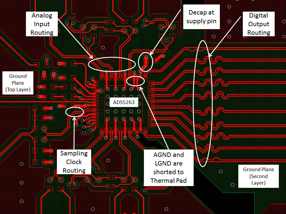
- At each power-supply pin (AVDD, DVDD, or AVDDD3V), keep a 0.1-µF de-coupling capacitor close to the device. A separate de-coupling capacitor group consisting of a parallel combination of 10-µF, 1-µF, and 0.1-µF capacitors can be kept close to the supply source.
- Use of a ground plane is recommended.
- Keep digital outputs away from the analog inputs. When these digital outputs exit the pinout, the digital output traces must not be kept parallel to the analog input traces because this configuration can result in coupling from the digital outputs to the analog inputs and degrade performance. All digital output traces to the receiver [such as a field-programmable gate array (FPGA) or an application-specific integrated circuit (ASIC)] must be matched in length to avoid skew among outputs.
Since ADS5263 provides charging current and system power with internal linear regulators, users need to consider thermal condition.
- PowerPAD should be soldered to a thermal land on the PCB.
- Vias on the thermal land of the PCB are necessary. This is a thermal path through the other side of the PCB.
- A thermal pad of the same size is required on the other side of the PCB. All thermal pads should be connected by vias.
- A metal layer should cover all of the PCB if possible.
- Place vias to connect other sides to create thermal paths.
With these steps, the thermal resistance of ADS5263 can be lowered.
