ZHCS190D May 2011 – November 2015 ADS5263
PRODUCTION DATA.
- 1 特性
- 2 应用
- 3 说明
- 4 修订历史记录
- 5 说明 (续)
- 6 Pin Configuration and Functions
-
7 Specifications
- 7.1 Absolute Maximum Ratings
- 7.2 ESD Ratings
- 7.3 Recommended Operating Conditions
- 7.4 Thermal Information
- 7.5 Electrical Characteristics, Dynamic Performance - 16-Bit ADC
- 7.6 Electrical Characteristics, General - 16-Bit ADC Mode
- 7.7 Electrical Characteristics, Dynamic Performance - 14-Bit ADC
- 7.8 Digital Characteristics
- 7.9 Timing Requirements
- 7.10 LVDS Timing at Lower Sampling Frequencies - 2 Wire, 8× Serialization
- 7.11 LVDS Timing for 1 Wire 16× Serialization
- 7.12 LVDS Timing for 2 Wire, 7× Serialization
- 7.13 LVDS Timing for 1 Wire, 14× Serialization
- 7.14 Serial Interface Timing Requirements
- 7.15 Reset Switching Characteristics
- 7.16 Typical Characteristics
-
8 Detailed Description
- 8.1 Overview
- 8.2 Functional Block Diagram
- 8.3 Feature Description
- 8.4 Device Functional Modes
- 8.5 Programming
- 8.6 Register Maps
- 9 Application and Implementation
- 10Power Supply Recommendations
- 11Layout
- 12器件和文档支持
- 13机械、封装和可订购信息
9 Application and Implementation
NOTE
Information in the following applications sections is not part of the TI component specification, and TI does not warrant its accuracy or completeness. TI’s customers are responsible for determining suitability of components for their purposes. Customers should validate and test their design implementation to confirm system functionality.
9.1 Application Information
ADS5263 is a high-performance 16-bit quad-channel ADC with sample rates up to 100 MSPS.
The conversion process is initiated by a rising edge of the external input clock and the analog input signal is sampled. The sampled signal is sequentially converted by a series of small resolution stages with the outputs combined in a digital correction logic block. At every clock edge the sample propagates through the pipeline, resulting in a data latency of 16 clock cycles. The output is available as 16-bit data in serial LVDS format, coded in either offset binary or binary 2s-complement format.
The device also has a 14-bit low-power mode, where it operates as a quad-channel 14-bit ADC. The 16-bit front-end stage is powered down and the part consumes almost half the power, compared to the 16-bit mode. The ADS5263 can be dynamically switched between the two resolution modes. This allows systems to use the same part in a high-resolution, high-power mode or a low-resolution, low-power mode.
The INxA pins are used as the 16-bit ADC inputs, and the INxB pins function as the 14-bit ADC inputs.
9.1.1 Analog Input
The analog input consists of a switched-capacitor based differential sample and hold architecture.
This differential topology results in very good ac performance, even for high input frequencies at high sampling rates. The INxP and INxM pins must be externally biased around a common-mode voltage of 1.5 V, available on the VCM pin. For a full-scale differential input, each input pin INP, INM must swing symmetrically between VCM + 1 V and VCM – 1 V, resulting in a 4-Vpp differential input swing.
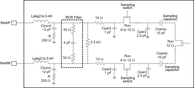 Figure 90. 16-Bit ADC – Analog Input Equivalent Circuit
9.1.1.1 Drive Circuit Requirements
For optimum performance, the analog inputs must be driven differentially. This improves the common-mode noise immunity and even-order harmonic rejection. A 5-Ω to 15-Ω resistor in series with each input pin is recommended to damp out ringing caused by package parasitics. It is also necessary to present low impedance ( <50 Ω) for the common mode switching currents. This can be achieved by using two resistors from each input terminated to the common mode voltage (VCM).
Note that the device includes an internal R-C-R filter across the input pins. The purpose of the filter is to absorb the glitches caused by the opening and closing of the sampling capacitors. The cutoff frequency of the R-C filter involves a trade-off. A lower cutoff frequency (larger C) absorbs glitches better, but also reduces the input bandwidth and the maximum input frequency that can be supported. On the other hand, with no internal R-C filter, high input frequency can be supported, but now the sampling glitches must be supplied by the external driving circuit. The inductance of the package bond wires limits the ability of the drive circuit to support these glitches.
Figure 91 and Figure 92 show the impedance (Zin = Rin || Cin) looking across the differential ADC input pins. While designing the external drive circuit, the ADC input impedance must be considered.
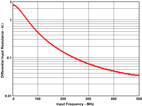 Figure 91. ADC Analog Input Resistance (Rin)
 Across Frequency
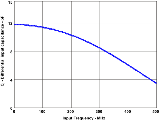 Figure 92. ADC Analog Input Capacitance (CIN)
 Across Frequency
9.1.2 Large and Small Signal Input Bandwidth
The small signal bandwidth of the analog input circuit is high, around 700 MHz. When using an amplifier to drive the ADS5263, the total noise of the amplifier up to the small signal bandwidth must be considered.
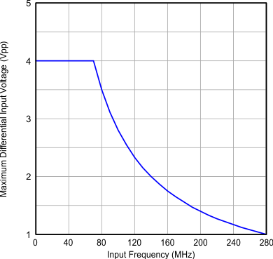
The large signal bandwidth of the device depends on the amplitude of the input signal. The ADS5263 supports 4 VPP amplitude for input signal frequency up to 70 MHz. For higher frequencies (>70 MHz), the amplitude of the input signal must be decreased proportionally. For example, at 140 MHz, the device supports a maximum of 2 VPP signal and at 280 MHz, it can handle a maximum of 1 VPP.
9.1.3 Clamp Function For CCD Signals
The 14-bit ADC analog inputs have an integrated clamp function that can be used to interface to a CCD sensor output.
9.1.3.1 Differential Input Drive
The clamp function can be used with a differential input signal only. As most CCD signals are single-ended, use either a fully differential amplifier or transformer to translate the single-ended CCD signal to a differential signal for applying to the ADS5263 analog inputs through ac-coupling capacitors, as Figure 94 shows.
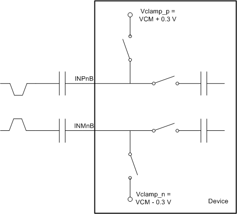 Figure 94. Differential Input Drive with Internal Clamp Mode
The analog inputs of the ADS5263 are internally clamped to voltages Vclamp_p (1.8 V, typical) and Vclamp_n (1.2 V, typical). With a differential input, the voltage on INP can swing from Vclamp_p down to 1 V, whereas INM swings from Vclamp_n up to 2 V. This ensures maintaining of the input common-mode at 1.5 V while supporting a differential input swing of 1.6 Vpp.
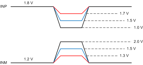 Figure 95. Analog Input Voltage Range With Clamp Enabled
9.1.3.2 Clamp Operation
The clamp function can be enabled by setting the register bit <EN_CLAMP> in register 0x09.
The effect of the clamp operation can be verified by measuring the voltage on the INP and INM pins. With no input signal applied, the voltages on INP and INM will be 1.8 V dc and 1.2 V dc, respectively.
9.1.3.3 Synchronization to External CCD Timing
A typical CCD sensor output has three timing phases – a reset phase followed by a reference phase and the actual picture phase.
An internally generated CLAMP clock signal controls the clamping action. The CLAMP clock can be timed to happen during the reset phase of the CCD signal by applying a synchronized high-going pulse on SYNC pin. Once synchronized, the internal CLAMP signal remains high for one ADC clock cycle and low for two clock cycles and repeats in this fashion. Figure 96 shows an oscilloscope snapshot of the external input signals applied to the ADS5263 and the alignment of the CCD signal to the SYNC input. shows the relation between the external signals, the internally generated CLAMP signal, and the data actually sampled by the ADC.
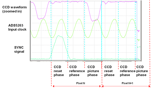 Figure 96. Synchronizing CCD Signal with ADS5263's Clamp Operation Using SYNC signal
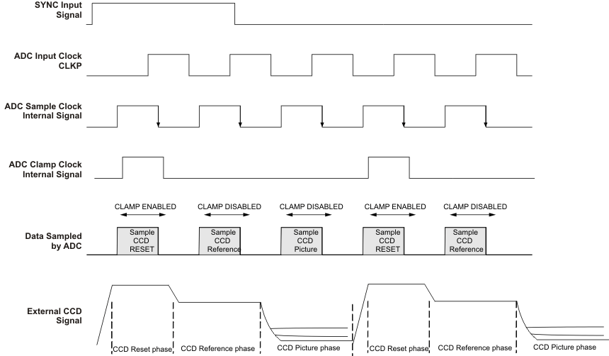 Clamp Timing Diagram
9.1.4 Low-Frequency Noise Suppression
The low-frequency noise suppression mode is specifically useful in applications where good noise performance is desired in the low frequency band of dc to 1 MHz. By setting this mode, the low-frequency noise spectrum band around dc is shifted to a similar band around (fS/2 or Nyquist frequency). As a result, the noise spectrum from dc to about 1 MHz improves significantly as shown by the following spectrum plots.
This function can be selectively enabled in each channel using the register bits <EN LFNS CH x>. The following plots show the effect of this mode on the spectrum.
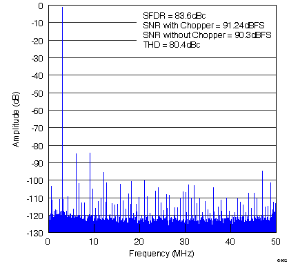 Figure 97. Full-Scale Input Amplitude
 with LF Noise Suppression Enabled_LAS760.png) Figure 99. Spectrum (Zoomed) in 1-MHz Band from 49 MHz to 50 MHz (fS=100 MSPS)
Figure 99. Spectrum (Zoomed) in 1-MHz Band from 49 MHz to 50 MHz (fS=100 MSPS)
 with LF Noise Suppression Enabled_LAS760.png) Figure 98. Spectrum (Zoomed) from DC to 1 MHz
Figure 98. Spectrum (Zoomed) from DC to 1 MHz
9.1.5 External Reference Mode
The ADS5263 supports an external reference mode of operation by applying an input voltage on VCM pin.
As shown in the figure, in this mode, the reference amplifier is still active. Instead of being driven by the internal band-gap voltage, the reference amplifier is driven by the voltage applied on the VCM pin. By driving the VCM pin with a low drift reference, it is possible to improve the reference temperature drift compared to the internal reference mode. The relation between the full-scale voltage of the ADC and the applied voltage on VCM is
Full-scale input voltage = (8/3) x VREFIN
To enable this mode, set the register bits as shown in Table 11. This changes the function of the VCM pin to an external reference input pin. The voltage applied on VCM must be 1.5 V ± 50 mV. The current drawn by VCM pin in this mode is around 0.5 mA.
Table 11. Register Settings for External Reference Mode
| REGISTER ADDRESS | FIELD NAME | VALUE |
|---|---|---|
| 0x01 | EN_HIGH_ADDRS | 1 |
| 0xF0 | EN_EXT_REF | 1 |
| 0x42 | EN_REG_42 | 1 |
| 0x42 | EXT_REF_VCM | 1 |
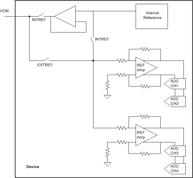 Figure 100. Reference Block Diagram
9.2 Typical Applications
9.2.1 Driving Circuit Design: Low Input Frequencies (< 50 MHz)
 Figure 101. Driving Circuit for Low Input Frequencies
9.2.1.1 Design Requirements
For optimum performance, the analog inputs must be driven differentially. An optional 5-Ω to 15-Ω resistor in series with each input pin can be kept to damp out ringing caused by package parasitics. The drive circuit may have to be designed to minimize the impact of kick-back noise generated by sampling switches opening and closing inside the ADC, as well as ensuring low insertion loss over the desired frequency range and matched impedance to the source.
9.2.1.2 Detailed Design Procedure
A typical application using two back-to-back coupled transformers is illustrated in Figure 101. The circuit is optimized for low input frequencies. An external R-C-C-R filter using 50-Ω resistors and a 27-pF capacitor is used. With the series inductor (39 nH), this combination helps absorb the sampling glitches.
9.2.1.3 Application Curve
Typical performance at full-scale 10 MHz input frequency is shown in Figure 102.
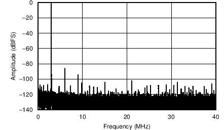
| fS = 80 MSPS, SNR = 85 dBFS, fIN = 3 MHz , SFDR = 83 dBc |
9.2.2 Driving Circuit Design: Input Frequencies > 50 MHz
 Figure 103. Driving Circuit for High Input Frequencies (fIN > 50 MHz)
9.2.2.1 Design Requirements
To achieve optimum performance at high input frequencies, an example driving circuit is shown in Figure 103.
9.2.2.2 Detailed Design Procedure
When input frequencies are greater than 50 MHz, series inductance from low frequency driving circuit should be removed so as not limit the signal bandwidth. The corner frequency of R-C-C-R low pass filter should also be changed to suit the input frequency.
9.2.2.3 Application Curve
Figure 104 shows the performance obtained by using the circuit shown in Figure 104.
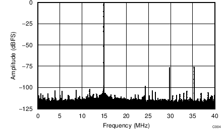
| fS = 80 MSPS, SNR = 78.2 dBFS, fIN = 65 MHz, SFDR = 75 dBc |
