ZHCSDS3C May 2015 – April 2018 ADS52J90
PRODUCTION DATA.
- 1 特性
- 2 应用
- 3 说明
- 4 修订历史记录
- 5 说明 (续)
- 6 Pin Configuration and Functions
-
7 Specifications
- 7.1 Absolute Maximum Ratings
- 7.2 ESD Ratings
- 7.3 Recommended Operating Conditions
- 7.4 Thermal Information
- 7.5 Electrical Characteristics
- 7.6 Digital Characteristics
- 7.7 Timing Requirements: Signal Chain
- 7.8 Timing Requirements: JESD Interface
- 7.9 Timing Requirements: Serial Interface
- 7.10 Typical Characteristics
- 7.11 Typical Characteristics: JESD Interface
- 7.12 Typical Characteristics: Contour Plots
-
8 Detailed Description
- 8.1 Overview
- 8.2 Functional Block Diagrams
- 8.3
Feature Description
- 8.3.1 Connection of the External Inputs to the Input Pins
- 8.3.2 Input Multiplexer and Sampler
- 8.3.3 Analog-to-Digital Converter (ADC)
- 8.3.4 Device Synchronization Using TX_TRIG
- 8.3.5 Digital Processing
- 8.3.6 Data Formatting
- 8.3.7 Serializer and LVDS Interface
- 8.3.8 LVDS Buffers
- 8.3.9 JESD204B Interface
- 8.3.10 Interfacing SYNC~ and SYSREF Between the FPGA and ADCs
- 8.3.11 Clock Input
- 8.3.12 Analog Input and Driving Circuit
- 8.4 Device Functional Modes
- 8.5 Programming
- 9 Application and Implementation
- 10Power Supply Recommendations
- 11Layout
-
12Register Map
- 12.1
ADC Registers
- 12.1.1
Description of Registers
- 12.1.1.1 Register 0h (address = 0h)
- 12.1.1.2 Register 1h (address = 1h)
- 12.1.1.3 Register 2h (address = 2h)
- 12.1.1.4 Register 3h (address = 3h)
- 12.1.1.5 Register 4h (address = 4h)
- 12.1.1.6 Register 5h (address = 5h)
- 12.1.1.7 Register 7h (address = 7h)
- 12.1.1.8 Register 8h (address = 8h)
- 12.1.1.9 Register Ah (address = Ah)
- 12.1.1.10 Register Bh (address = Bh)
- 12.1.1.11 Register Dh (address = Dh)
- 12.1.1.12 Register Eh (address = Eh)
- 12.1.1.13 Register Fh (address = Fh)
- 12.1.1.14 Register 10h (address = 10h)
- 12.1.1.15 Register 11h (address = 11h)
- 12.1.1.16 Register 12h (address = 12h)
- 12.1.1.17 Register 13h (address = 13h)
- 12.1.1.18 Register 14h (address = 14h)
- 12.1.1.19 Register 15h (address = 15h)
- 12.1.1.20 Register 17h (address = 17h)
- 12.1.1.21 Register 18h (address = 18h)
- 12.1.1.22 Register 19h (address = 19h)
- 12.1.1.23 Register 1Ah (address = 1Ah)
- 12.1.1.24 Register 1Bh (address = 1Bh)
- 12.1.1.25 Register 1Ch (address = 1Ch)
- 12.1.1.26 Register 1Dh (address = 1Dh)
- 12.1.1.27 Register 1Eh (address = 1Eh)
- 12.1.1.28 Register 1Fh (address = 1Fh)
- 12.1.1.29 Register 20h (address = 20h)
- 12.1.1.30 Register 21h (offset = 21h)
- 12.1.1.31 Register 23h (register = 23h)
- 12.1.1.32 Register 24h (address = 24h)
- 12.1.1.33 Register 25h (address = 25h)
- 12.1.1.34 Register 26h (address = 26h)
- 12.1.1.35 Register 27h (address = 27h)
- 12.1.1.36 Register 28h (address = 28h)
- 12.1.1.37 Register 29h (address = 29h)
- 12.1.1.38 Register 2Ah (address = 2Ah)
- 12.1.1.39 Register 2Bh (address = 2Bh)
- 12.1.1.40 Register 2Ch (address = 2Ch)
- 12.1.1.41 Register 2Dh (address = 2Dh)
- 12.1.1.42 Register 2Fh (address = 2Fh)
- 12.1.1.43 Register 30h (address = 30h)
- 12.1.1.44 Register 31h (address = 31h)
- 12.1.1.45 Register 32h (address = 32h)
- 12.1.1.46 Register 33h (address = 33h)
- 12.1.1.47 Register 34h (address = 34h)
- 12.1.1.48 Register 35h (address = 35h)
- 12.1.1.49 Register 36h (address = 36h)
- 12.1.1.50 Register 37h (address = 37h)
- 12.1.1.51 Register 38h (address = 38h)
- 12.1.1.52 Register 39h (address = 39h)
- 12.1.1.53 Register 3Bh (address = 3Bh)
- 12.1.1.54 Register 3Ch (address = 3Ch)
- 12.1.1.55 Register 43h (address = 43h)
- 12.1.1
Description of Registers
- 12.2
JESD Serial Interface Registers
- 12.2.1
Description of JESD Serial Interface Registers
- 12.2.1.1 Register 70 (address = 46h)
- 12.2.1.2 Register 73 (address = 49h)
- 12.2.1.3 Register 74 (address = 4Ah)
- 12.2.1.4 Register 75 (address = 4Bh)
- 12.2.1.5 Register 77 (address = 4Dh)
- 12.2.1.6 Register 80 (address = 50h)
- 12.2.1.7 Register 81 (address = 51h)
- 12.2.1.8 Register 82 (address = 52h)
- 12.2.1.9 Register 83 (address = 53h)
- 12.2.1.10 Register 85 (address = 55h)
- 12.2.1.11 Register 115 (address = 73h)
- 12.2.1.12 Register 116 (address = 74h)
- 12.2.1.13 Register 117 (address = 75h)
- 12.2.1.14 Register 118 (address = 76h)
- 12.2.1.15 Register 119 (address = 77h)
- 12.2.1.16 Register 120 (address = 78h)
- 12.2.1.17 Register 134 (address = 86h)
- 12.2.1.18 Register 135 (address = 87h)
- 12.2.1.19 Register 136 (address = 88h)
- 12.2.1.20 Register 137 (address = 89h)
- 12.2.1.21 Register 138 (address = 8Ah)
- 12.2.1
Description of JESD Serial Interface Registers
- 12.1
ADC Registers
- 13器件和文档支持
- 14机械、封装和可订购信息
8.3.2 Input Multiplexer and Sampler
The input multiplexer determines the mapping of the input pins (IN1 to IN32) to the inputs that are sampled and converted by the ADCs (ADC1 to ADC16). Each ADC has two sets of sampling circuits (termed odd and even) and alternately converts the inputs presented to them.
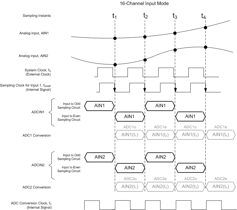
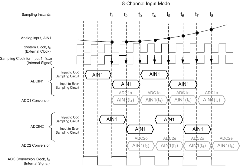
The sampling windows for the odd and even sampling circuits of each ADC are derived from the system clock. A pair of ADCs are used in Figure 57, Figure 58, and Figure 59 to illustrate how the odd and even sampling phases are derived for each ADC in each input mode. AIN1 (t1) refers to the AIN1 input sampled at the t1 instant. ADC1o refers to the odd sample converted by ADC1 and ADC1e refers to the even sample converted by ADC1. The input sampling and conversion schemes for the 32-, 16-, and 8-input modes are illustrated in Figure 57, Figure 58, and Figure 59, respectively.
 Figure 57. Input Sampling and Conversion Scheme (32-Input Mode)
 Figure 58. Input Sampling and Conversion Scheme (16-Input Mode)
 Figure 59. Input Sampling and Conversion Scheme (8-Input Mode)
Mapping the inputs of the odd and even sampling circuits of subsequent-numbered ADCs to subsequent-numbered sets of input pairs repeats in a similar manner.
The sampling rate (fSAMP) can be defined as the rate at which the device converts each analog input presented to it. The relationship between the sampling rate and the system clock frequency is listed in Table 2 for the three input modes.
Table 2. Sampling Rate and Input Clock Frequency
| ANALOG INPUT MODE (Number of Input Channels) | SAMPLING RATE (fSAMP) |
|---|---|
| 16 | fS |
| 32 | 0.5 × fS |
| 8 | fS |
In 16-input mode, each ADC converts one input at a sampling rate equal to the system clock. In 32-input mode, one ADC alternately converts two sets of inputs, each at a sampling rate that is half the system clock. In the 8-input mode, two ADCs convert the same input in interleaved manner.
In 16-input mode, a ping-pong operation exists between two sampling circuits of one ADC that are sampling the same input. The mismatch between the two sampling circuit bandwidths can result in an interleaving spur at
(fS / 2 ± fIN), where fS is the frequency of the system clock and fIN is the frequency of the input signal.
In 8-input mode, additional interleaving across two adjacent ADCs is present in addition to the ping-pong operation between the two sampling circuits of the same ADC. This increased mismatch can result in significant interleaving spurs at (fS / 2 ± fIN) and (fS / 4 ± fIN). The offset mismatch between the four sets of sampling circuits can result in a spur at fS / 4.
For the 32-input mode, the sampling instants of the even-numbered input signals are offset from the sampling instants of the odd-numbered input signals by one system clock period. The magnitude of the interleaving spurs increases when the input frequency is increased because the sampling bandwidth mismatch across the different sampling circuits results in larger phase error mismatches when the input frequency is increased.