SLAS669E September   2010  – may 2020 ADS5400-SP

PRODUCTION DATA.  

  1. Features
  2. Applications
  3. Description
    1.     Block Diagram
  4. Revision History
  5. Pin Configuration and Functions
    1.     Pin Functions
  6. Specifications
    1. 6.1 Absolute Maximum Ratings
    2. 6.2 ESD Ratings
    3. 6.3 Recommended Operating Conditions
    4. 6.4 Thermal Information
    5. 6.5 Electrical Characteristics
    6. 6.6 Switching Characteristics
    7. 6.7 Timing Characteristics
    8. 6.8 Interleaving Adjustments
    9. 6.9 Typical Characteristics
  7. Detailed Description
    1. 7.1 Overview
    2. 7.2 Functional Block Diagram
    3. 7.3 Feature Description
      1. 7.3.1  Input Configuration
      2. 7.3.2  Voltage Reference
      3. 7.3.3  Analog Input Over-Range Recovery Error
      4. 7.3.4  Clock Inputs
      5. 7.3.5  Over Range
      6. 7.3.6  Data Scramble
      7. 7.3.7  Test Patterns
      8. 7.3.8  Die Identification and Revision
      9. 7.3.9  Die Temperature Sensor
      10. 7.3.10 Interleaving
        1. 7.3.10.1 Gain Adjustment
        2. 7.3.10.2 Offset Adjustment
        3. 7.3.10.3 Input Clock Coarse Phase Adjustment
        4. 7.3.10.4 Input Clock Fine Phase Adjustment
    4. 7.4 Device Functional Modes
      1. 7.4.1 Output Bus and Clock Options
      2. 7.4.2 Reset and Synchronization
      3. 7.4.3 LVDS
    5. 7.5 Programming
      1. 7.5.1 Serial Interface
        1. Table 2. Instruction Byte of the Serial Interface
    6. 7.6 Serial Register Map
      1. 7.6.1 Description of Serial Registers
  8. Application and Implementation
    1. 8.1 Application Information
    2. 8.2 Typical Application
      1. 8.2.1 Design Requirements
      2. 8.2.2 Detailed Design Procedure
        1. 8.2.2.1 Clocking Source for ADS5400-SP
        2. 8.2.2.2 Amplifier Selection
      3. 8.2.3 Application Curve
  9. Power Supply Recommendations
  10. 10Layout
    1. 10.1 Layout Guidelines
    2. 10.2 Layout Example
  11. 11Device and Documentation Support
    1. 11.1 Device Support
      1. 11.1.1 Device Nomenclature
        1. 11.1.1.1 Definition of Specifications
    2. 11.2 Documentation Support
    3. 11.3 Receiving Notification of Documentation Updates
    4. 11.4 Support Resources
    5. 11.5 Trademarks
    6. 11.6 Electrostatic Discharge Caution
    7. 11.7 Glossary
  12. 12Mechanical, Packaging, and Orderable Information

封装选项

机械数据 (封装 | 引脚)
散热焊盘机械数据 (封装 | 引脚)
订购信息

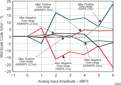
Analog Input Over-Range Recovery Error

An over-range condition occurs if the analog input voltage exceeds the full-scale range of the converter (0dBFS). To test recovery from an over-range, the ADC analog input is injected with a sinusoidal input frequency exactly at CLKIN/4 (a four-point sinusoid at the digital outputs). The four sample points of each period occur at the top, mid-scale, bottom and mid-scale of the sinusoid (clipped by the ADC when over-ranged to all 0s or all 1s). Once the amplitude exceeds 0dBFS, the top and bottom of the sinusoidal input becomes out of range, while the mid-scale point is always in-range and measureable with ADC output codes. The graph in Figure 27 indicates the amount of error from the expected mid-scale value of 2048 that occurs after negative over-range (bottom of sinusoid) and positive over-range (top of sinusoid). This equates to the amount of error in a valid sample 1 clock cycle after an over-range occurs, as a function of input amplitude.
ADS5400-SP G023_LAS611.gifFigure 27. Recovery Error 1 Clock Cycle After Over-Range vs Input Amplitude