SLAS669E September 2010 – may 2020 ADS5400-SP
PRODUCTION DATA.
- 1 Features
- 2 Applications
- 3 Description
- 4 Revision History
- 5 Pin Configuration and Functions
- 6 Specifications
-
7 Detailed Description
- 7.1 Overview
- 7.2 Functional Block Diagram
- 7.3 Feature Description
- 7.4 Device Functional Modes
- 7.5 Programming
- 7.6 Serial Register Map
- 8 Application and Implementation
- 9 Power Supply Recommendations
- 10Layout
- 11Device and Documentation Support
- 12Mechanical, Packaging, and Orderable Information
6.8 Interleaving Adjustments
Typical values at TA = 25°C, Min and Max values over full temperature range TMIN = –55°C to TMAX = 125°C,sampling rate = 1 GSPS, 50% clock duty cycle, AVDD5 = 5 V, AVDD3 = 3.3 V, DVDD3 = 3.3 V, and 1.5 VPP differential clock (unless otherwise noted)
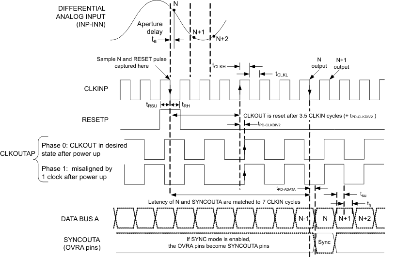
Propagation delays and setup/hold times not drawn to scale. RESET and SYNCOUT are optional. Any clock phase will work properly, but makes synchronization of data capture across multiple ADCs difficult without a known CLKOUT phase. RESET can be a single pulse (as shown), low-to-high step or repetitive pulse input signal. The frequency of repetitive RESET pulses should not exceed CLKIN/2, and should be an even divisor of CLKIN, in order to keep the CLKOUT phase the same with each RESET event. SYNCOUTA transitions with the same latency as the sample that is present when the RESET pulse is captured, shown here as sample N. Each RESET captured generates a SYNCOUT pulse, which behaves as a data bit. Bus B is not active in single bus mode.
Figure 1. Single Bus Mode 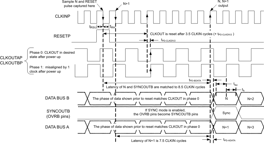
Propagation delays and setup/hold times not drawn to scale. RESET and SYNCOUT are optional. Any clock phase will work properly, but makes synchronization of data capture across multiple ADCs difficult without a known CLKOUT phase. RESET can be a single pulse (as shown), low-to-high step or repetitive pulse input signal. The frequency of repetitive RESET pulses should not exceed CLKIN/2, and should be an even divisor of CLKIN, in order to keep the CLKOUT phase the same with each RESET event. SYNCOUTB transitions with the same latency as the sample that is present when the RESET pulse is captured, shown here as sample N. Each RESET captured generates a SYNCOUT pulse, which behaves as a data bit.
Figure 2. Dual Bus Mode - Aligned, CLKOUT Divide By 2 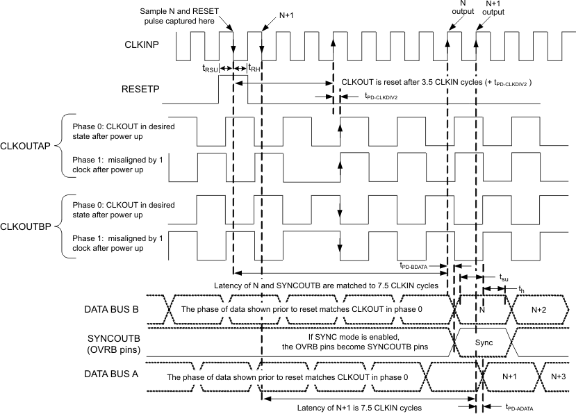
Propagation delays and setup/hold times not drawn to scale. RESET and SYNCOUT are optional. Any clock phase will work properly, but makes synchronization of data capture across multiple ADCs difficult without a known CLKOUT phase. RESET can be a single pulse (as shown), low-to-high step or repetitive pulse input signal. The frequency of repetitive RESET pulses should not exceed CLKIN/2, and should be an even divisor of CLKIN, in order to keep the CLKOUT phase the same with each RESET event. SYNCOUTB transitions with the same latency as the sample that is present when the RESET pulse is captured, shown here as sample N. Each RESET captured generates a SYNCOUT pulse, which behaves as a data bit.
Figure 3. Dual Bus Mode - Staggered, CLKOUT Divide By 2 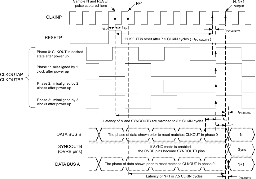
Propagation delays and setup/hold times not drawn to scale. RESET and SYNCOUT are optional. Any clock phase will work properly, but makes synchronization of data capture across multiple ADCs difficult without a known CLKOUT phase. RESET can be a single pulse (as shown), low-to-high step or repetitive pulse input signal. The frequency of repetitive RESET pulses should not exceed CLKIN/4, and should be an even divisor of CLKIN, in order to keep the CLKOUT phase the same with each RESET event. SYNCOUTB transitions with the same latency as the sample that is present when the RESET pulse is captured, shown here as sample N. Each RESET captured generates a SYNCOUT pulse, which behaves as a data bit.
Figure 4. Dual Bus Mode - Aligned, CLKOUT Divide By 4 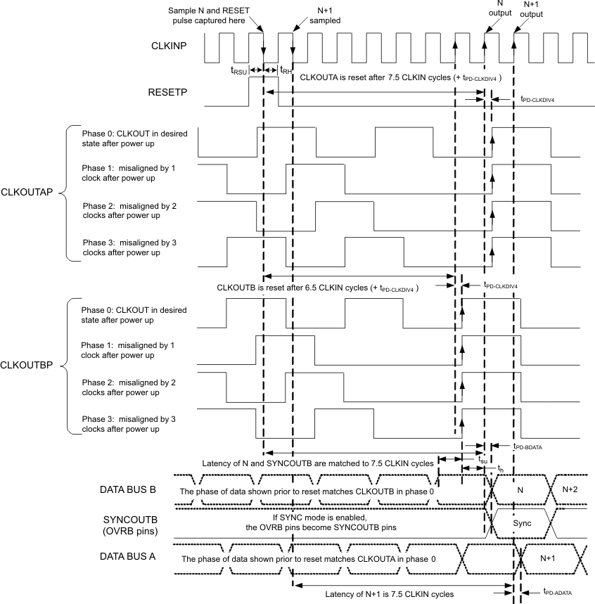
Propagation delays and setup/hold times not drawn to scale. RESET and SYNCOUT are optional. Any clock phase will work properly, but makes synchronization of data capture across multiple ADCs difficult without a known CLKOUT phase. RESET can be a single pulse (as shown), low-to-high step or repetitive pulse input signal. The frequency of repetitive RESET pulses should not exceed CLKIN/4, and should be an even divisor of CLKIN, in order to keep the CLKOUT phase the same with each RESET event. SYNCOUTB transitions with the same latency as the sample that is present when the RESET pulse is captured, shown here as sample N. Each RESET captured generates a SYNCOUT pulse, which behaves as a data bit.
Figure 5. Dual Bus Mode - Staggered, CLKOUT Divide By 4