SLAS669E September   2010  – may 2020 ADS5400-SP

PRODUCTION DATA.  

  1. Features
  2. Applications
  3. Description
    1.     Block Diagram
  4. Revision History
  5. Pin Configuration and Functions
    1.     Pin Functions
  6. Specifications
    1. 6.1 Absolute Maximum Ratings
    2. 6.2 ESD Ratings
    3. 6.3 Recommended Operating Conditions
    4. 6.4 Thermal Information
    5. 6.5 Electrical Characteristics
    6. 6.6 Switching Characteristics
    7. 6.7 Timing Characteristics
    8. 6.8 Interleaving Adjustments
    9. 6.9 Typical Characteristics
  7. Detailed Description
    1. 7.1 Overview
    2. 7.2 Functional Block Diagram
    3. 7.3 Feature Description
      1. 7.3.1  Input Configuration
      2. 7.3.2  Voltage Reference
      3. 7.3.3  Analog Input Over-Range Recovery Error
      4. 7.3.4  Clock Inputs
      5. 7.3.5  Over Range
      6. 7.3.6  Data Scramble
      7. 7.3.7  Test Patterns
      8. 7.3.8  Die Identification and Revision
      9. 7.3.9  Die Temperature Sensor
      10. 7.3.10 Interleaving
        1. 7.3.10.1 Gain Adjustment
        2. 7.3.10.2 Offset Adjustment
        3. 7.3.10.3 Input Clock Coarse Phase Adjustment
        4. 7.3.10.4 Input Clock Fine Phase Adjustment
    4. 7.4 Device Functional Modes
      1. 7.4.1 Output Bus and Clock Options
      2. 7.4.2 Reset and Synchronization
      3. 7.4.3 LVDS
    5. 7.5 Programming
      1. 7.5.1 Serial Interface
        1. Table 2. Instruction Byte of the Serial Interface
    6. 7.6 Serial Register Map
      1. 7.6.1 Description of Serial Registers
  8. Application and Implementation
    1. 8.1 Application Information
    2. 8.2 Typical Application
      1. 8.2.1 Design Requirements
      2. 8.2.2 Detailed Design Procedure
        1. 8.2.2.1 Clocking Source for ADS5400-SP
        2. 8.2.2.2 Amplifier Selection
      3. 8.2.3 Application Curve
  9. Power Supply Recommendations
  10. 10Layout
    1. 10.1 Layout Guidelines
    2. 10.2 Layout Example
  11. 11Device and Documentation Support
    1. 11.1 Device Support
      1. 11.1.1 Device Nomenclature
        1. 11.1.1.1 Definition of Specifications
    2. 11.2 Documentation Support
    3. 11.3 Receiving Notification of Documentation Updates
    4. 11.4 Support Resources
    5. 11.5 Trademarks
    6. 11.6 Electrostatic Discharge Caution
    7. 11.7 Glossary
  12. 12Mechanical, Packaging, and Orderable Information

封装选项

机械数据 (封装 | 引脚)
散热焊盘机械数据 (封装 | 引脚)
订购信息

Power Supply Recommendations

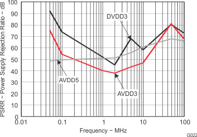
The ADS5400-SP uses three power supplies. For the analog portion of the design, a 5-V and 3.3-V supply (AVDD5 and AVDD3) are used, while the digital portion uses a 3.3-V supply (DVDD3). The use of low-noise power supplies with adequate decoupling is recommended. Linear supplies are preferred to switched supplies; switched supplies generate more noise components that can be coupled to the ADS5400-SP. The PSRR value and the plot shown in Figure 41 were obtained without bulk supply decoupling capacitors. When bulk (0.1 μF) decoupling capacitors are used, the board-level PSRR is much higher than the stated value for the ADC. The power consumption of the device does not change substantially over clock rate or input frequency as a result of the architecture and process.
ADS5400-SP G022_LAS611.gifFigure 41. PSRR versus Supply Injected Frequency