SLAS611C October 2009 – January 2016 ADS5400
PRODUCTION DATA.
- 1 Features
- 2 Applications
- 3 Description
- 4 Revision History
- 5 Pin Configuration and Functions
- 6 Specifications
-
7 Detailed Description
- 7.1 Overview
- 7.2 Functional Block Diagram
- 7.3 Feature Description
- 7.4 Device Functional Modes
- 7.5 Programming
- 7.6 Register Maps
- 8 Application and Implementation
- 9 Power Supply Recommendations
- 10Layout
- 11Device and Documentation Support
- 12Mechanical, Packaging, and Orderable Information
封装选项
机械数据 (封装 | 引脚)
- PZP|100
散热焊盘机械数据 (封装 | 引脚)
- PZP|100
订购信息
6 Specifications
6.1 Absolute Maximum Ratings
over operating free-air temperature range (unless otherwise noted)(1)| MIN | MAX | UNIT | ||||
|---|---|---|---|---|---|---|
| Supply voltage | AVDD5 to GND | 6 | V | |||
| AVDD3 to GND | 5 | V | ||||
| DVDD3 to GND | 5 | V | ||||
| AINP, AINN to GND(2) | Voltage difference between pin and ground | 0.5 | 4.5 | V | ||
| AINP to AINN(2) | Voltage difference between pins, common mode at AVDD5/2 | Short duration | –0.3 | (AVDD5 + 0.3) | V | |
| Continuous AC signal | 1.25 | 3.75 | V | |||
| Continuous DC signal | 1.75 | 3.25 | V | |||
| Pin voltage | CLKINP, CLKINN to GND(2) | Voltage difference between pin and ground | 0.5 | 4.5 | V | |
| CLKINP to CLKINN(2) | Voltage difference between pins, common mode at AVDD5/2 | Continuous AC signal | 1.1 | 3.9 | V | |
| Continuous DC signal | 2 | 3 | V | |||
| RESETP, RESETN to GND(2) | Voltage difference between pin and ground | –0.3 | (AVDD5 + 0.3) | V | ||
| RESETP to RESETN(2) | Voltage difference between pins | Continuous AC signal | 1.1 | 3.9 | V | |
| Continuous DC signal | 2 | 3 | V | |||
| Data/OVR Outputs to GND(2) | Voltage difference between pin and ground | –0.3 | (DVDD3 + 0.3) | V | ||
| SDENB, SDIO, SCLK to GND(2) | –0.3 | (AVDD3 + 0.3) | ||||
| ENA1BUS, ENPWD, ENEXTREF to GND(2) | –0.3 | (AVDD5 + 0.3) | ||||
| Temperature | Operating | –40 | 85 | °C | ||
| Maximum junction , TJ | 150 | °C | ||||
| Storage, Tstg | –65 | 150 | °C | |||
(1) Stresses above these ratings may cause permanent damage. Exposure to absolute maximum conditions for extended periods may degrade device reliability. These are stress ratings only, and functional operation of the device at these or any other conditions beyond those specified is not implied. Kirkendall voidings and current density information for calculation of expected lifetime is available upon request.
(2) Valid when supplies are within recommended operating range.
6.2 ESD Ratings
| VALUE | UNIT | |||
|---|---|---|---|---|
| V(ESD) | Electrostatic discharge | Human body model (HBM), per ANSI/ESDA/JEDEC JS-001(1) | 2000 | V |
| Charged device model (CDM), per JEDEC specification JESD22-C101(2) | 500 | |||
(1) JEDEC document JEP155 states that 500-V HBM allows safe manufacturing with a standard ESD control process.
(2) JEDEC document JEP157 states that 250-V CDM allows safe manufacturing with a standard ESD control process.
6.3 Recommended Operating Conditions
6.4 Thermal Information
| THERMAL METRIC(1) | ADS5400 | UNIT | |
|---|---|---|---|
| PZP (HTQFP) | |||
| 100 PINS | |||
| RθJA | Junction-to-ambient thermal resistance | 34.5 | °C/W |
| RθJC(top) | Junction-to-case (top) thermal resistance | 7.4 | °C/W |
| RθJB | Junction-to-board thermal resistance | 9.1 | °C/W |
| ψJT | Junction-to-top characterization parameter | 0.2 | °C/W |
| ψJB | Junction-to-board characterization parameter | 9 | °C/W |
| RθJC(bot) | Junction-to-case (bottom) thermal resistance | 0.4 | °C/W |
(1) For more information about traditional and new thermal metrics, see the Semiconductor and IC Package Thermal Metrics application report, SPRA953.
6.5 Electrical Characteristics
Typical values at TA = 25°C, minimum and maximum values over full temperature range TMIN = –40°C to TMAX = 85°C, sampling rate = 1 GSPS, 50% clock duty cycle, AVDD5 = 5 V, AVDD3 = 3.3 V, DVDD3 = 3.3 V, –1-dBFS differential input, and 1.5 VPP differential clock (unless otherwise noted)| PARAMETER | TEST CONDITIONS | MIN | TYP | MAX | UNIT | |
|---|---|---|---|---|---|---|
| ANALOG INPUTS | ||||||
| Full-scale differential input range | Programmable | 1.52 | 2 | VPP | ||
| VCM | Common-mode input | Self-biased to AVDD5 / 2 | AVDD5/2 | V | ||
| RIN | Input resistance, differential (DC) | 85 | 100 | 115 | Ω | |
| CIN | Input capacitance | Estimated to ground from each AIN pin, excluding soldered package | 0.8 | pF | ||
| CMRR | Common-mode rejection ratio | Common mode signal = 125 MHz | 40 | dB | ||
| INTERNAL REFERENCE VOLTAGE | ||||||
| VREF | Reference voltage | 2 | V | |||
| DYNAMIC ACCURACY | ||||||
| Resolution | No missing codes | 12 | Bits | |||
| DNL | Differential linearity error | fIN = 125 MHz | –1 | ±0.7 | 2 | LSB |
| INL | Integral non- linearity error | fIN = 125 MHz | –4 | ±2 | 4.5 | LSB |
| Offset error | default is trimmed near 0 mV | –2.5 | 0 | 2.5 | mV | |
| Offset temperature coefficient | 0.02 | mV /°C | ||||
| Gain error | –5 | 5 | % full scale | |||
| Gain temperature coefficient | 0.03 | % full scale /°C | ||||
| POWER SUPPLY(1) | ||||||
| I(AVDD5) | 5-V analog supply current (Bus A and B active) | fIN = 125 MHz, fS = 1 GSPS |
220 | 234 | mA | |
| 5-V analog supply current (Bus A active) | fIN = 125 MHz, fS = 1 GSPS |
225 | 241 | mA | ||
| I(AVDD3) | 3.3-V analog supply current (Bus A and B active) | fIN = 125 MHz, fS = 1 GSPS |
219 | 234 | mA | |
| 3.3-V analog supply current (Bus A active) | fIN = 125 MHz, fS = 1 GSPS |
226 | 242 | mA | ||
| I(DVDD3) | 3.3-V digital supply current (Bus A and B active) |
fIN = 125 MHz, fS = 1 GSPS |
136 | 154 | mA | |
| 3.3-V digital supply current (Bus A active) |
fIN = 125 MHz, fS = 1 GSPS |
71 | 81 | mA | ||
| Total power dissipation (BUS A and B active) |
fIN = 125 MHz, fS = 1 GSPS |
2.28 | 2.45 | W | ||
| Total power dissipation (Bus A active) |
fIN = 125 MHz, fS = 1 GSPS |
2.15 | 2.25 | W | ||
| Total power dissipation | ENPWD = logic High (sleep enabled) | 13 | 50 | mW | ||
| Wake-up time from sleep | 1.8 | ms | ||||
| PSRR | Power-supply rejection ratio | 1MHz injected to each supply, measured without external decoupling | 50 | dB | ||
| DYNAMIC AC CHARACTERISTICS | ||||||
| SNR | Signal-to-noise ratio | fIN = 125 MHz | 57 | 58.5 | dBFS | |
| fIN = 600 MHz | 56.5 | 58.2 | ||||
| fIN = 850 MHz | 56 | 57.8 | ||||
| fIN = 1200 MHz | 57.6 | |||||
| fIN = 1700 MHz | 55.7 | |||||
| SFDR | Spurious-free dynamic range | fIN = 125 MHz | 65 | 75 | dBc | |
| fIN = 600 MHz | 63 | 72 | ||||
| fIN = 850 MHz | 60 | 71 | ||||
| fIN = 1200 MHz | 66 | |||||
| fIN = 1700 MHz | 56 | |||||
| HD2 | Second harmonic | fIN = 125 MHz | 65 | 78 | dBc | |
| fIN = 600 MHz | 63 | 78 | ||||
| fIN = 850 MHz | 60 | 71 | ||||
| fIN = 1200 MHz | 66 | |||||
| fIN = 1700 MHz | 56 | |||||
| HD3 | Third harmonic | fIN = 125 MHz | 65 | 80 | dBc | |
| fIN = 600 MHz | 63 | 72 | ||||
| fIN = 850 MHz | 60 | 72 | ||||
| fIN = 1200 MHz | 70 | |||||
| fIN = 1700 MHz | 65 | |||||
| Worst harmonic/spur (other than HD2 and HD3) | fIN = 125 MHz | 65 | 80 | dBc | ||
| fIN = 600 MHz | 63 | 72 | ||||
| fIN = 850 MHz | 60 | 72 | ||||
| fIN = 1200 MHz | 66 | |||||
| fIN = 1700 MHz | 64 | |||||
| THD | Total Harmonic Distortion | fIN = 125 MHz | 63 | 71.7 | dBc | |
| fIN = 600 MHz | 62 | 67 | ||||
| fIN = 850 MHz | 59 | 66.5 | ||||
| fIN = 1200 MHz | 65.1 | |||||
| fIN = 1700 MHz | 55.7 | |||||
| SINAD | Signal-to-noise and distortion | fIN = 125 MHz | 56 | 58.5 | dBFS | |
| fIN = 600 MHz | 55 | 58.2 | ||||
| fIN = 850 MHz | 54 | 57.8 | ||||
| fIN = 1200 MHz | 57.5 | |||||
| fIN = 1700 MHz | 54.2 | |||||
| Two-tone SFDR | fIN1 = 247.5 MHz, fIN2 = 252.5 MHz, each tone at –7 dBFS | 74.6 | dBFS | |||
| fIN1 = 247.5 MHz, fIN2 = 252.5 MHz, each tone at –11 dBFS | 80.4 | |||||
| fIN1 = 1197.5 MHz, fIN2 = 1202.5 MHz, each tone at –7 dBFS | 70 | |||||
| fIN1 = 1197.5 MHz, fIN2 = 1202.5 MHz, each tone at –11 dBFS | 78.3 | |||||
| ENOB | Effective number of bits (using SINAD in dBFS) | fIN = 125 MHz | 9 | 9.42 | Bits | |
| fIN = 600 MHz | 8.84 | 9.37 | ||||
| fIN = 850 MHz | 8.67 | 9.3 | ||||
| RMS idle-channel noise | Inputs tied to common-mode | 1.41 | LSB rms | |||
| 60.2 | dBFS | |||||
(1) All power values assume LVDS output current is set to 3.5 mA.
6.6 Interleaving Adjustments
Typical values at TA = 25°C, Minimum and maximum values over full temperature range TMIN = –40°C to TMAX = 85°C, sampling rate = 1 GSPS, 50% clock duty cycle, AVDD5 = 5 V, AVDD3 = 3.3 V, DVDD3 = 3.3 V, and 1.5 VPP differential clock (unless otherwise noted)6.7 Timing Requirements
Typical values at TA = 25°C, Minimum and maximum values over full temperature range TMIN = –40°C to TMAX = 85°C, sampling rate = 1 GSPS, 50% clock duty cycle, AVDD5 = 5 V, AVDD3 = 3.3 V, DVDD3 = 3.3 V, and 1.5 VPP differential clock (unless otherwise noted)(1).| MIN | NOM | MAX | UNIT | ||||
|---|---|---|---|---|---|---|---|
| ta | Aperture delay | 250 | ps | ||||
| Aperture jitter, rms | Uncertainty of sample point due to internal jitter sources | 125 | fs | ||||
| Latency | Bus A, using Single Bus Mode | 7 | Cycles | ||||
| Bus A, using Dual Bus Mode Aligned | 7.5 | ||||||
| Bus B, using Dual Bus Mode Aligned | 8.5 | ||||||
| Bus A and B, using Dual Bus Mode Staggered | 7.5 | ||||||
| LVDS OUTPUT TIMING (DATA, CLKOUT, OVR/SYNCOUT)(2) | |||||||
| tCLK | Clock period | 1 | 10 | ns | |||
| tCLKH | Clock pulse duration, high | Assuming worst case 45/55 duty cycle | 0.45 | ns | |||
| tCLKL | Clock pulse duration, low | Assuming worst case 55/45 duty cycle | 0.45 | ns | |||
| tPD-CLKDIV2 | Clock propagation delay | CLKIN rising to CLKOUT rising in divide by 2 mode | 700 | 1200 | 1700 | ps | |
| tPD-CLKDIV4 | Clock propagation delay | CLKIN rising to CLKOUT rising in divide by 4 mode | 700 | 1200 | 1700 | ps | |
| tPD-ADATA | Bus A data propagation delay | CLKIN falling to Data Output transition | 700 | 1400 | 2100 | ps | |
| tPD-BDATA | Bus B data propagation delay | CLKIN falling to Data Output transition | 700 | 1400 | 2100 | ps | |
| tSU-SBM (3) | Setup time, single bus mode | Data valid to CLKOUT edge, 50% CLKIN duty cycle | 290p | (tCLK/2) - 185p | s | ||
| tH-SBM | Hold time, single bus mode | CLKOUT edge to Data invalid, 50% CLKIN duty cycle | 410p | (tCLK/2) - 65p | s | ||
| tSU-DBM | Setup time, dual bus mode | Data valid to CLKOUT edge, 50% CLKIN duty cycle | 550p | tCLK - 425p | s | ||
| tH-DBM | Hold time, dual bus mode | CLKOUT edge to Data invalid, 50% CLKIN duty cycle | 1150p | tCLK + 175p | s | ||
| tr | LVDS rise time | Measured 20% to 80% | 400 | ps | |||
| tf | LVDS output fall time | Measured 20% to 80% | 400 | ps | |||
| LVDS INPUT TIMING (RESETIN) | |||||||
| tRSU | RESET setup time | RESETP going HIGH to CLKINP going LOW | 300 | ps | |||
| tRH | RESET hold time | CLKINP going LOW to RESETP going LOW | 300 | ps | |||
| RESET input capacitance | Differential | 1 | pF | ||||
| RESET input current | ±1 | µA | |||||
| SERIAL INTERFACE TIMING | |||||||
| tS-SDENB | Setup time, serial enable | SDENB falling to SCLK rising | 20 | ns | |||
| tH-SDENB | Hold time, serial enable | SCLK falling to SENDB rising | 25 | ns | |||
| tS-SDIO | Setup time, SDIO | SDIO valid to SCLK rising | 10 | ns | |||
| tH-SDIO | Hold time, SDIO | SCLK rising to SDIO transition | 10 | ns | |||
| fSCLK | Frequency | 10 | MHz | ||||
| tSCLK | SCLK period | 100 | ns | ||||
| tSCLKH | Minimum SCLK high time | 40 | ns | ||||
| tSCLKL | Minimum SCLK low time | 40 | ns | ||||
| tr | Rise time | 10 pF | 10 | ns | |||
| tf | Fall time | 10 pF | 10 | ns | |||
| tDDATA | Data output delay | Data output (SDO/SDIO) delay after SCLK falling, 10-pF load | 75 | ns | |||
(1) Timing parameters are specified by design or characterization, but not production tested.
(2) LVDS output timing measured with a differential 100-Ω load placed ~4 inches from the ADS5400. Measured differential load capacitance is 3.5 pF. Measurement probes and other parasitics add ~1 pF. Total approximate capacitive load is 4.5 pF differential. All timing parameters are relative to the device pins, with the loading as stated.
(3) In single bus mode at 1 GSPS (1-ns clock), the minimum output setup/hold times over process and temperature provide a minimum 700 ps of data valid window, with 300 ps of uncertainity.
6.8 Switching Characteristics
Typical values at TA = 25°C, Minimum and maximum values over full temperature range TMIN = –40°C to TMAX = 85°C, sampling rate = 1 GSPS, 50% clock duty cycle, AVDD5 = 5 V, AVDD3 = 3.3 V, DVDD3 = 3.3 V, and 1.5 VPP differential clock (unless otherwise noted)| PARAMETER | TEST CONDITIONS | MIN | TYP | MAX | UNIT | |
|---|---|---|---|---|---|---|
| LVDS DIGITAL OUTPUTS (DATA, OVR/SYNCOUT, CLKOUT) | ||||||
| VOD | Differential output voltage (±) | Terminated 100 Ω differential | 247 | 350 | 454 | mV |
| VOC | Common mode output voltage | Terminated 100 Ω differential | 1.125 | 1.25 | 1.375 | V |
| LVDS DIGITAL INPUTS (RESET) | ||||||
| VID | Differential input voltage (±) | Each input pin | 175 | 350 | mV | |
| VIC | Common mode input voltage | Each input pin | 0.1 | 1.25 | 2.4 | V |
| RIN | Input resistance | 85 | 100 | 115 | Ω | |
| CIN | Input capacitance | Each pin to ground | 0.6 | pF | ||
| DIGITAL INPUTS (SCLK, SDIO, SDENB) | ||||||
| VIH | High level input voltage | 2 | AVDD3 + 0.3 | V | ||
| VIL | Low level input voltage | 0 | 0.8 | V | ||
| IIH | High level input current | ±1 | μA | |||
| IIL | Low level input current | ±1 | μA | |||
| CIN | Input capacitance | 2 | pF | |||
| DIGITAL INPUTS ( ENEXTREF, ENPWD, ENA1BUS) | ||||||
| VIH | High level input voltage | 2 | AVDD5 + 0.3 | V | ||
| VIL | Low level input voltage | 0 | 0.8 | V | ||
| IIH | High level input current | ~40-kΩ internal pulldown | 125 | μA | ||
| IIL | Low level input current | ~40-kΩ internal pulldown | 20 | μA | ||
| CIN | Input capacitance | 2 | pF | |||
| DIGITAL OUTPUTS (SDIO, SDO) | ||||||
| VOH | High level output voltage | IOH = 250 µA | 2.8 | V | ||
| VOL | Low level output voltage | IOL = 250 µA | 0.4 | V | ||
| CLOCK INPUTS | ||||||
| RIN | Differential input resistance | CLKINP, CLKINN | 130 | 160 | 190 | Ω |
| CIN | Input capacitance | Estimated to ground from each CLKIN pin, excluding soldered packaged | 0.8 | pF | ||
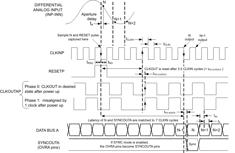
Propagation delays and setup/hold times not drawn to scale. RESET and SYNCOUT are optional. Any clock phase will work properly, but makes synchronization of data capture across multiple ADCs difficult without a known CLKOUT phase. RESET can be a single pulse (as shown), low-to-high step or repetitive pulse input signal. The frequency of repetitive RESET pulses should not exceed CLKIN/2, and should be an even divisor of CLKIN, to keep the CLKOUT phase the same with each RESET event. SYNCOUTA transitions with the same latency as the sample that is present when the RESET pulse is captured, shown here as sample N. Each RESET captured generates a SYNCOUT pulse, which behaves as a data bit. Bus B is not active in single bus mode.
Figure 1. Single Bus Mode
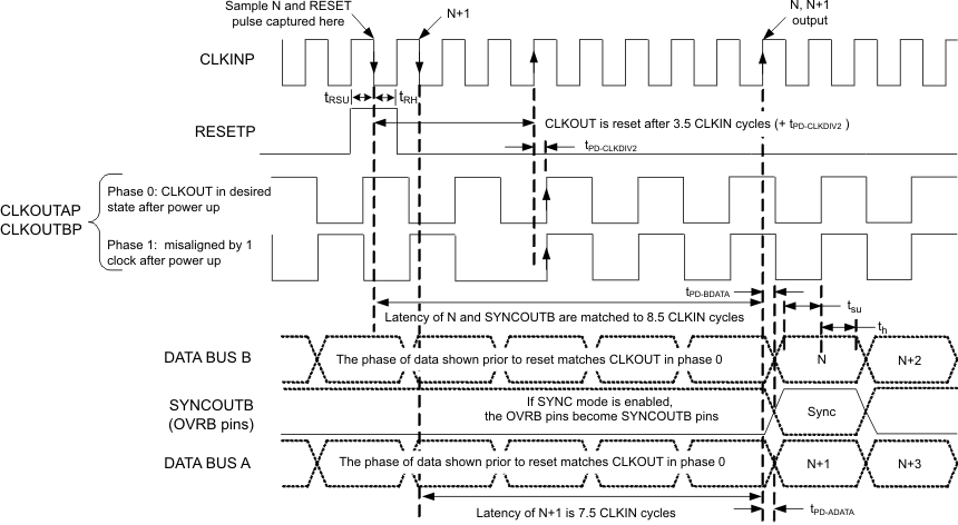
Propagation delays and setup/hold times not drawn to scale. RESET and SYNCOUT are optional. Any clock phase will work properly, but makes synchronization of data capture across multiple ADCs difficult without a known CLKOUT phase. RESET can be a single pulse (as shown), low-to-high step or repetitive pulse input signal. The frequency of repetitive RESET pulses should not exceed CLKIN/2, and should be an even divisor of CLKIN, to keep the CLKOUT phase the same with each RESET event. SYNCOUTB transitions with the same latency as the sample that is present when the RESET pulse is captured, shown here as sample N. Each RESET captured generates a SYNCOUT pulse, which behaves as a data bit.
Figure 2. Dual Bus Mode - Aligned, CLKOUT Divide By 2
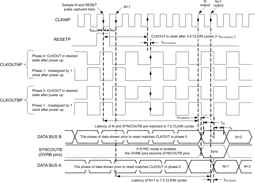
Propagation delays and setup/hold times not drawn to scale. RESET and SYNCOUT are optional. Any clock phase will work properly, but makes synchronization of data capture across multiple ADCs difficult without a known CLKOUT phase. RESET can be a single pulse (as shown), low-to-high step or repetitive pulse input signal. The frequency of repetitive RESET pulses should not exceed CLKIN/2, and should be an even divisor of CLKIN, to keep the CLKOUT phase the same with each RESET event. SYNCOUTB transitions with the same latency as the sample that is present when the RESET pulse is captured, shown here as sample N. Each RESET captured generates a SYNCOUT pulse, which behaves as a data bit.
Figure 3. Dual Bus Mode - Staggered, CLKOUT Divide By 2
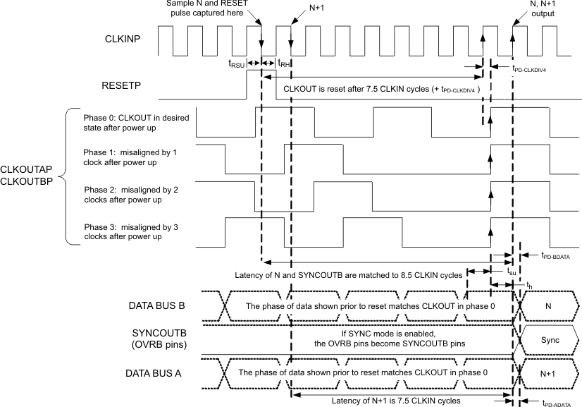
Propagation delays and setup/hold times not drawn to scale. RESET and SYNCOUT are optional. Any clock phase will work properly, but makes synchronization of data capture across multiple ADCs difficult without a known CLKOUT phase. RESET can be a single pulse (as shown), low-to-high step or repetitive pulse input signal. The frequency of repetitive RESET pulses should not exceed CLKIN/4, and should be an even divisor of CLKIN, to keep the CLKOUT phase the same with each RESET event. SYNCOUTB transitions with the same latency as the sample that is present when the RESET pulse is captured, shown here as sample N. Each RESET captured generates a SYNCOUT pulse, which behaves as a data bit.
Figure 4. Dual Bus Mode - Aligned, CLKOUT Divide By 4
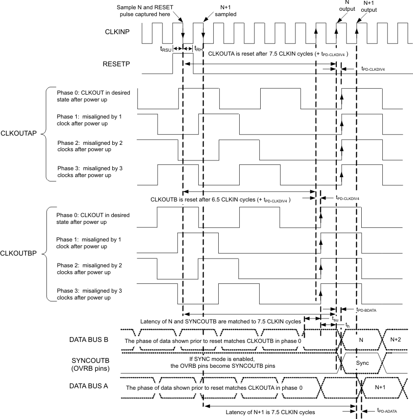
Propagation delays and setup/hold times not drawn to scale. RESET and SYNCOUT are optional. Any clock phase will work properly, but makes synchronization of data capture across multiple ADCs difficult without a known CLKOUT phase. RESET can be a single pulse (as shown), low-to-high step or repetitive pulse input signal. The frequency of repetitive RESET pulses should not exceed CLKIN/4, and should be an even divisor of CLKIN, to keep the CLKOUT phase the same with each RESET event. SYNCOUTB transitions with the same latency as the sample that is present when the RESET pulse is captured, shown here as sample N. Each RESET captured generates a SYNCOUT pulse, which behaves as a data bit.
Figure 5. Dual Bus Mode - Staggered, CLKOUT Divide By 4
6.9 Typical Characteristics
Typical plots at TA = 25°C, sampling rate = 1 GSPS, 50% clock duty cycle, AVDD5 = 5 V, AVDD3 = 3.3 V, DVDD3 = 3.3 V, and 1.5-VPP differential clock, (unless otherwise noted)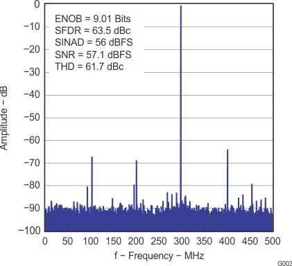 Figure 8. Spectral Performance FFT for 1.3-GHz Input Signal
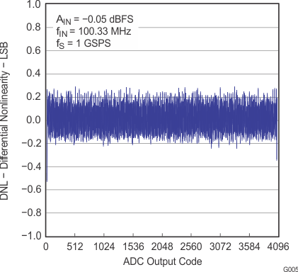 Figure 10. Differential Nonlinearity
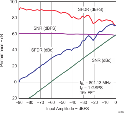 Figure 12. AC Performance vs Input Amplitude
(801.13-MHz Input Signal)
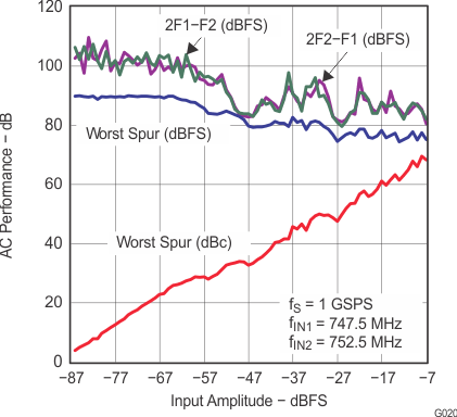 Figure 14. AC Performance vs Input Amplitude
(747.5-MHz and 752.5-MHz Two-Tone Input Signal)
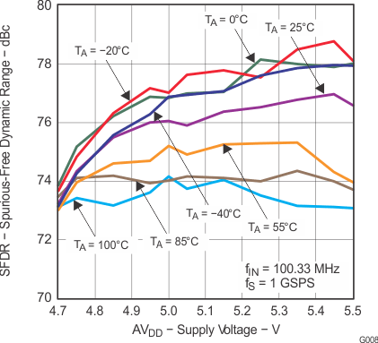 Figure 16. SFDR vs AVDD5 Across Temperature
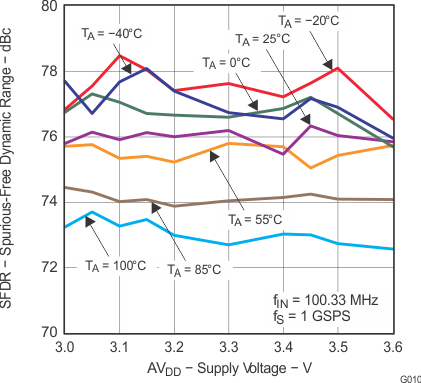 Figure 18. SFDR vs AVDD3 Across Temperature
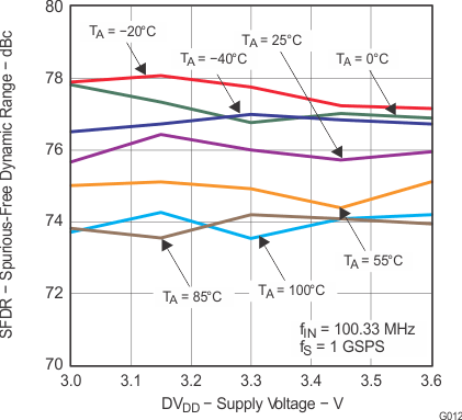 Figure 20. SFDR vs DVDD3 Across Temperature
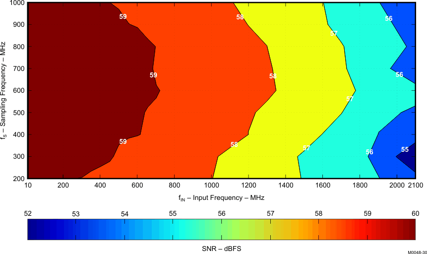 Figure 22. SNR vs Input Frequency and Sampling Frequency
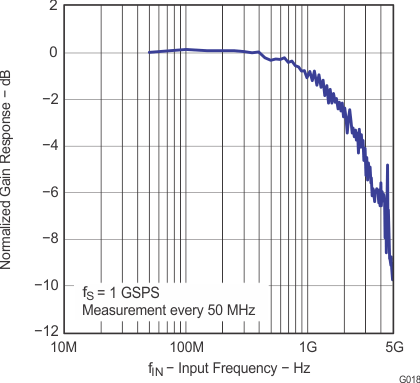 Figure 24. Normalized Gain Response vs Input Frequency
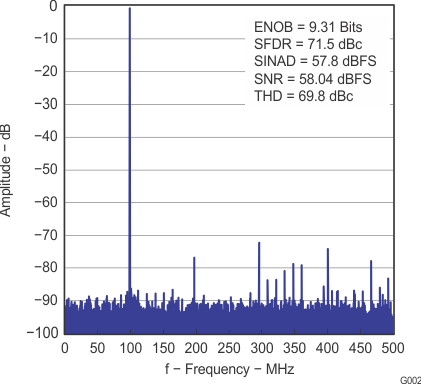 Figure 7. Spectral Performance FFT for 0.9-GHz Input Signal
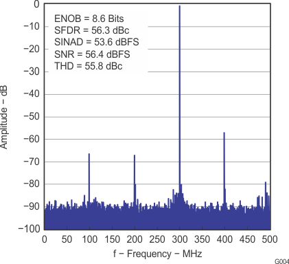 Figure 9. Spectral Performance FFT for 1.7-GHz Input Signal
 Figure 11. Integral Nonlinearity
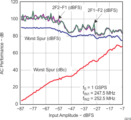 Figure 13. AC Performance vs Input Amplitude
(247.5-MHz and 252.5-MHz Two-Tone Input Signal)
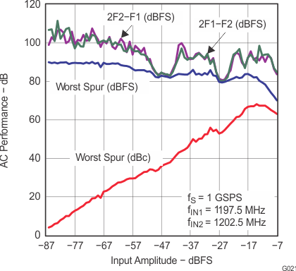 Figure 15. AC Performance vs Input Amplitude
(1197.5-MHz and 1202.5-MHz Two-Tone Input Signal)
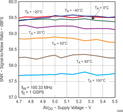 Figure 17. SNR vs AVDD5 Across Temperature
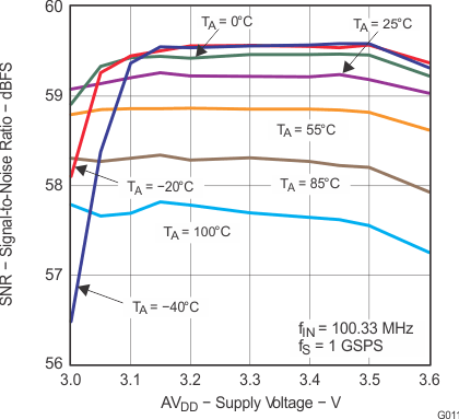 Figure 19. SNR vs AVDD3 Across Temperature
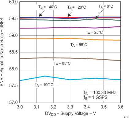 Figure 21. SNR vs DVDD3 Across Temperature
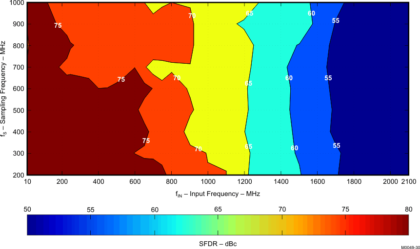 Figure 23. SFDR vs Input Frequency and Sampling Frequency
