ZHCSAV9B April 2013 – January 2016 ADS5401
PRODUCTION DATA.
- 1 特性
- 2 应用
- 3 说明
- 4 修订历史记录
- 5 Device Options
- 6 Pin Configuration and Functions
-
7 Specifications
- 7.1 Absolute Maximum Ratings
- 7.2 ESD Ratings
- 7.3 Recommended Operating Conditions
- 7.4 Thermal Information
- 7.5 Electrical Characteristics - Supply, Power Supply
- 7.6 Electrical Characteristics - Analog Inputs, Dynamic Accuracy, Clock Input
- 7.7 Electrical Characteristics - Dynamic AC, Enabled
- 7.8 Electrical Characteristics- Dynamic AC, Disabled
- 7.9 Electrical Characteristics - Over-Drive Recovery Error, Sample Timing
- 7.10 Electrical Characteristics - Digital Inputs, Digital Outputs
- 7.11 Serial Register Write Timing Requirements
- 7.12 Reset Timing Requirements
- 7.13 Typical Characteristics
-
8 Detailed Description
- 8.1 Overview
- 8.2 Functional Block Diagram
- 8.3 Feature Description
- 8.4 Device Functional Modes
- 8.5 Programming
- 8.6
Register Maps
- 8.6.1 Register Name: Config0 - Address: 0×00, Default = 0×00
- 8.6.2 Register Name: Config1 - Address: 0×01, Default = 0×00
- 8.6.3 Register Name: Config2 - Address: 0×02, Default = 0×780
- 8.6.4 Register Name: 3 - Address: 0x03
- 8.6.5 Register Name: E - Address: 0x0E
- 8.6.6 Register Name: F - Address: 0x0F
- 8.6.7 Register Name: 2B - Address: 0x2B
- 8.6.8 Register Name: 2C - Address: 0x2C
- 8.6.9 Register Name: 37 - Address: 0x37
- 8.6.10 Register Name: 38 - Address: 0x38
- 8.6.11 Register Name: 3A - Address: 0x3A
- 8.6.12 Register Name: 66 - Address: 0x66
- 9 Application and Implementation
- 10Power Supply Recommendations
- 11Layout
- 12器件和文档支持
- 13机械、封装和可订购信息
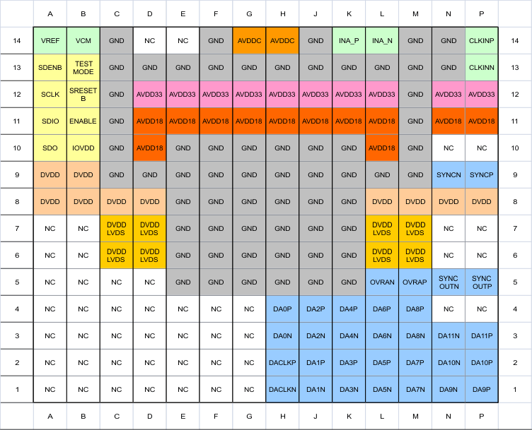
6 Pin Configuration and Functions
ZAY Package
196-Pin NFBGA
Top View

Pin Functions
| PIN | I/O | DESCRIPTION | |
|---|---|---|---|
| NAME | NO. | ||
| INPUT/REFERENCE | |||
| INA_P/N | K14, L14 | I | Analog ADC A differential input signal. |
| VCM | B14 | O | Output of the analog input common-mode (nominally 1.9 V). A 0.1-μF capacitor to AGND is recommended. |
| VREF | A14 | O | Reference voltage output (2-V nominal). A 0.1-μF capacitor to AGND is recommended, but not required. |
| CLOCK/SYNC | |||
| CLKINP/N | P14, P13 | I | Differential input clock |
| SYNCP/N | P9, N9 | I | Synchronization input. Inactive if logic low. When clocked in a high state initially, this is used for resetting internal clocks and digital logic and starting the SYNCOUT signal. Internal 100-Ω termination. |
| CONTROL/SERIAL | |||
| ENABLE | B11 | I | Chip enable – active high. Power-down function can be controlled through SPI register assignment. Internal 50-kΩ pullup resistor to IOVDD. |
| SCLK | A12 | I | Serial interface clock. Internal 50-kΩ pulldown resistor. |
| SDENB | A13 | I | Serial interface enable. Internal 50-kΩ pulldown resistor. |
| SDIO | A11 | I/O | Bidirectional serial data in 3 pin mode (default). In 4-pin interface mode (register x00, D16), the SDIO pin is an input only. Internal 50-kΩ pulldown. |
| SDO | A10 | O | Unidirectional serial interface data in 4 pin mode (register x00, D16). The SDO pin is tri-stated in 3-pin interface mode (default). Internal 50-kΩ pulldown resistor. |
| SRESET | B12 | I | Serial interface reset input. Active low. Initialized internal registers during high to low transition. Asynchronous. Internal 50-kΩ pullup resistor to IOVDD. |
| TESTMODE | B13 | — | Factory internal test, do not connect |
| DATA INTERFACE | |||
| DA[11:0]P/N | P3, N3, P2, N2, P1, N1, M4, M3, M2, M1, L4, L3, L2, L1, K4, K3, K2, K1, J4, J3, J2, J1, H4, H3 | O | ADC A Data Bits 11 (MSB) to 0 (LSB) in DDR output mode. Standard LVDS output. |
| DACLKP/N | H2, H1 | O | DDR differential output data clock for Bus A. Register programmable to provide either rising or falling edge to center of stable data nominal timing. |
| OVRAP/N | M5, L5 | O | Bus A, Overrange indicator, LVDS output. A logic high signals an analog input in excess of the full-scale range. Optional SYNC output. |
| NC | A1, A2, A3, A4, A5, A6, A7, B1, B2, B3, B4, B5, B6, B7, C1, C2, C3, C4, C5, D1, D2, D3, D4, D5, D14, E1, E2, E3, E4, E14, F3, F4, G1, G2, G3, G4, N4, N6, N7, N10, P4, P6, P7, P10 | — | Do not connect to pin |
| SYNCOUTP/N | F2, F1, P5, N5 | O | Synchronization output signal for synchronizing multiple ADCs. Can be disabled through SPI. |
| POWER SUPPLY | |||
| AVDD18 | D10, D11, E11, F11, G11, H11, J11, K11, L10, L11, N11, P11 | I | 1.8-V analog supply |
| AVDD33 | D12, E12, F12, G12, H12, J12, K12, L12, N12, P12 | I | 3.3-V analog supply |
| AVDDC | G14, H14 | I | 1.8-V supply for clock input |
| DVDD | A8, A9, B8, B9, C8, D8, L8, M8, N8, P8 | I | 1.8-V supply for digital block |
| DVDDLVDS | C6, C7, D6, D7, L6, L7, M6, M7 | I | 1.8-V supply for LVDS outputs |
| GND | I | Ground | |
| IOVDD | B10 | I | 1.8-V for digital I/Os |