SGLS378G March 2008 – October 2017 ADS5463-SP
PRODUCTION DATA.
- 1 Features
- 2 Applications
- 3 Description
- 4 Revision History
- 5 Pin Configuration and Functions
-
6 Specifications
- 6.1 Absolute Maximum Ratings
- 6.2 ESD Ratings
- 6.3 Recommended Operating Conditions
- 6.4 Thermal Information
- 6.5 Electrical Characteristics: ADS5463-RHA
- 6.6 Electrical Characteristics: ADS5463-RHA
- 6.7 Electrical Characteristics: ADS5463-RHA
- 6.8 Electrical Characteristics: ADS5463-SP
- 6.9 Electrical Characteristics: ADS5463-SP
- 6.10 Electrical Characteristics: ADS5463-SP
- 6.11 Timing Requirements
- 6.12 Typical Characteristics
- 7 Detailed Description
- 8 Application and Implementation
- 9 Power Supply Recommendations
- 10Layout
- 11Device and Documentation Support
- 12Mechanical, Packaging, and Orderable Information
10 Layout
10.1 Layout Guidelines
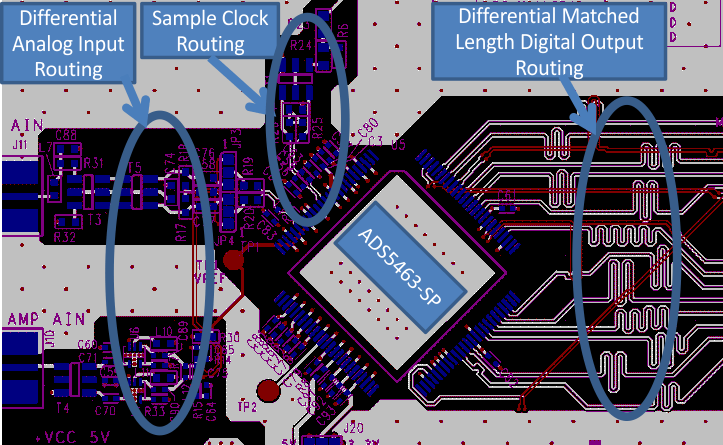
The evaluation board represents a good guideline of how to lay out the board to obtain the maximum performance from the ADS5463. General design rules, such as the use of multilayer boards, single ground plane for ADC ground connections, and local decoupling ceramic chip capacitors, should be applied. The input traces should be isolated from any external source of interference or noise, including the digital outputs as well as the clock traces. The clock signal traces also should be isolated from other signals, especially in applications where low jitter is required like high IF sampling. Besides performance-oriented rules, care must be taken when considering the heat dissipation of the device.
10.2 Layout Example
 Figure 22. Typical Layout of ADS5463-SP