SLAS525D July 2007 – December 2017 ADS5474
PRODUCTION DATA.
7 Detailed Description
7.1 Overview
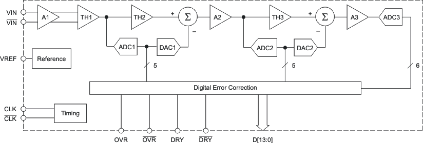
The ADS5474 device is a 14-bit, 400-MSPS, monolithic pipeline ADC. The bipolar analog core operates from 5-V and 3.3-V supplies, while the output uses a 3.3-V supply to provide LVDS-compatible outputs. The conversion process is initiated by the rising edge of the external input clock. At that instant, the differential input signal is captured by the input track-and-hold (T&H), and the input sample is converted sequentially by a series of lower resolution stages, with the outputs combined in a digital correction logic block. Both the rising and the falling clock edges are used to propagate the sample through the pipeline every half clock cycle. This process results in a data latency of 3.5 clock cycles, after which the output data are available as a 14-bit parallel word, coded in offset binary format.
7.2 Functional Block Diagram
7.3 Feature Description
The analog input for the ADS5474 device consists of an analog pseudo-differential buffer followed by a bipolar transistor T&H. The analog buffer isolates the source driving the input of the ADC from any internal switching and presents a high impedance that is easy to drive at high input frequencies, compared to an ADC without a buffered input. The input common-mode is set internally through a 500-Ω resistor connected from 3.1 V to each of the inputs (common-mode is approximately 2.4 V on 12-bit and 13-bit members of this family). This configuration results in a differential input impedance of 1 kΩ.
 Figure 34. Analog Input Equivalent Circuit
For a full-scale differential input, each of the differential lines of the input signal (pins 16 and 17) swings symmetrically between (3.1 V + 0.55 V) and (3.1 V – 0.55 V). This range means that each input has a maximum signal swing of 1.1 VPP for a total differential input signal swing of 2.2 VPP. Operation below 2.2 VPP is allowable, with the characteristics of performance versus input amplitude demonstrated in Figure 18 and Figure 19. For instance, for performance at 1.1 VPP rather than 2.2 VPP, refer to the SNR and SFDR at –6 dBFS (0 dBFS = 2.2 VPP). The maximum swing is determined by the internal reference voltage generator, eliminating the need for any external circuitry for this purpose.
7.3.1 Clock Inputs
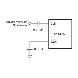
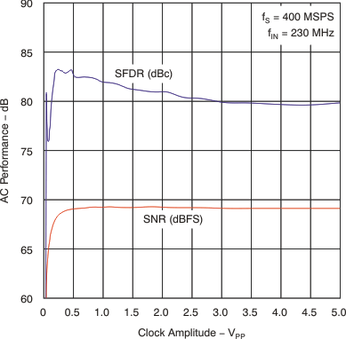
The ADS5474 device clock input can be driven with either a differential clock signal or a single-ended clock input. The characterization of the ADS5474 device is typically performed with a 3-VPP differential clock, but the ADC performs well with a differential clock amplitude down to approximately 0.5 VPP, as shown in Figure 37. The clock amplitude becomes more of a factor in performance as the analog input frequency increases. In low-input-frequency applications, where jitter may not be a big concern, the use of a single-ended clock could save cost and board space without much performance tradeoff. When clocked with this configuration, it is best to connect CLK to ground with a 0.01-μF capacitor, while CLK is ac-coupled with a 0.01-μF capacitor to the clock source, as shown in Figure 36.
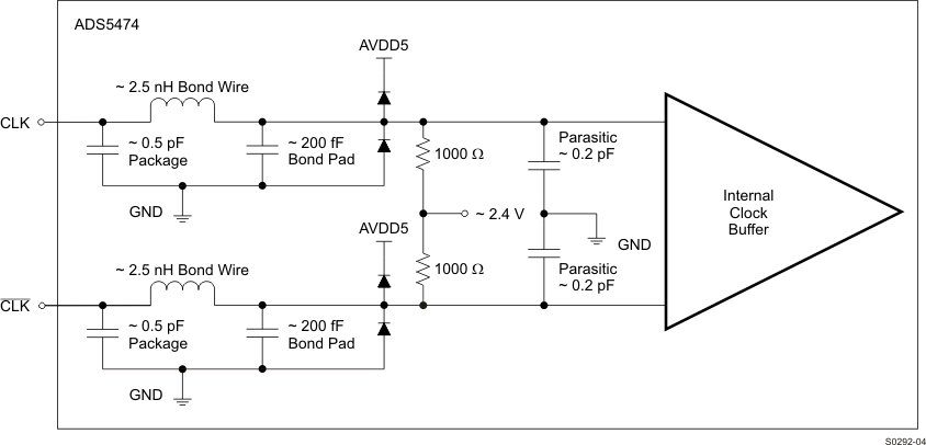 Figure 35. Clock Input Circuit
7.3.2 Digital Outputs
The ADC provides 14 LVDS-compatible, offset binary data outputs (D13 to D0; D13 is the MSB and D0 is the LSB), a data-ready signal (DRY), and an over-range indicator (OVR). TI recommends using the DRY signal to capture the output data of the ADS5474 device. DRY is source-synchronous to the DATA/OVR outputs and operates at the same frequency, creating a half-rate DDR interface that updates data on both the rising and falling edges of DRY. It is recommended that the capacitive loading on the digital outputs be minimized. Higher capacitance shortens the data-valid timing window. The values given for timing (see Figure 1) were obtained with a measured 10-pF parasitic board capacitance to ground on each LVDS line (or 5-pF differential parasitic capacitance). When setting the time relationship between DRY and DATA at the receiving device, it is generally recommended that setup time be maximized, but this partially depends on the setup and hold times of the device receiving the digital data (like an FPGA or Field Programmable Field Array). Since DRY and DATA are coincident, it will likely be necessary to delay either DRY or DATA such that setup time is maximized.
Referencing Figure 1, the polarity of DRY with respect to the sample N data output transition is undetermined because of the unknown startup logic level of the clock divider that generates the DRY signal (DRY is a frequency divide-by-two of CLK). Either the rising or the falling edge of DRY will be coincident with sample N and the polarity of DRY could invert when power is cycled off, on or when the power-down pin is cycled. Data capture from the transition and not the polarity of DRY is recommended, but not required. If the synchronization of multiple ADS5474 devices is required, it might be necessary to use a form of the CLKIN signal rather than DRY to capture the data.
The DRY frequency is identical on the ADS5474 and ADS5463 devices (where DRY equals ½ the CLK frequency), but different on the pin-similar ADS5444 and ADS5440 devices (where DRY equals the CLK frequency). The LVDS outputs all require an external 100-Ω load between each output pair in order to meet the expected LVDS voltage levels. For long trace lengths, it may be necessary to place a 100-Ω load on each digital output as close to the ADS5474 device as possible and another 100-Ω differential load at the end of the LVDS transmission line to provide matched impedance and avoid signal reflections. The effective load in this case reduces the LVDS voltage levels by half.
The OVR output equals a logic high when the 14-bit output word attempts to exceed either all 0s or all 1s. This flag is provided as an indicator that the analog input signal exceeded the full-scale input limit of approximately 2.2 VPP (± gain error). The OVR indicator is provided for systems that use gain control to keep the analog input signal within acceptable limits.
7.4 Device Functional Modes
7.4.1 External Voltage Reference
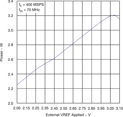
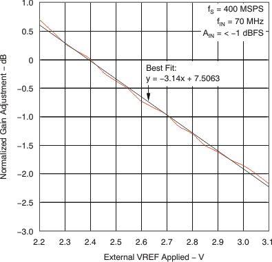
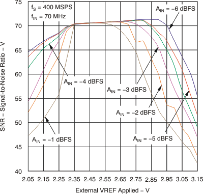
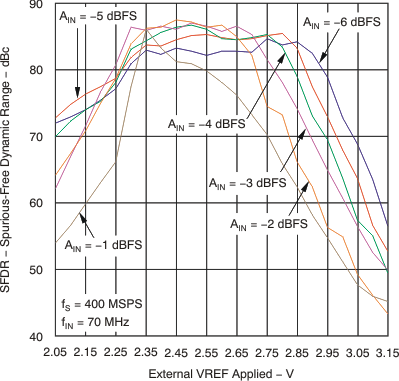
For systems that require the analog signal gain to be adjusted or calibrated, this can be performed by using an external reference. The dependency on the signal amplitude to the value of the external reference voltage is characterized typically by Figure 38 (VREF = 2.4 V is normalized to 0 dB as this is the internal reference voltage). As can be seen in the linear fit, this equates to approximately –0.3 dB of signal adjustment per 100 mV of reference adjustment. The range of allowable variation depends on the analog input amplitude that is applied to the inputs and the desired spectral performance, as can be seen in the performance versus external reference graphs in Figure 39 and Figure 40. As the applied analog signal amplitude is reduced, more variation in the reference voltage is allowed in the positive direction (which equates to a reduction in signal amplitude), whereas an adjustment in reference voltage below the nominal 2.4 V (which equates to an increase in signal amplitude) is not recommended below approximately 2.35 V. The power consumption versus reference voltage and operating temperature should also be considered, especially at high ambient temperatures, because the lifetime of the device is affected by internal junction temperature (see Figure 48).
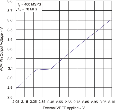
For dc-coupled applications that use the VCM pin of the ADS5474 device as the common mode of the signal in the analog signal gain path prior to the ADC inputs, the information in Figure 42 is useful to consider versus the allowable common-mode range of the device that is receiving the VCM voltage, such as an operational amplifier. Because it is pin-compatible, it is important to note that the ADS5463 does not have a VCM pin and primarily uses the VREF pin to provide the common-mode voltage in dc-coupled applications. The ADS5463 (VCM = 2.4 V) and ADS5474 (VCM = 3.1 V) devices do not have the same common-mode voltage. To create a board layout that may accommodate both devices in dc-coupled applications, route VCM and VREF both to a common point that can be selected via a switch, jumper, or a 0-Ω resistor.
