ZHCSF28B May 2016 – January 2017 ADS54J20
PRODUCTION DATA.
- 1 特性
- 2 应用
- 3 说明
- 4 修订历史记录
- 5 Device Comparison Table
- 6 Pin Configuration and Functions
- 7 Specifications
-
8 Detailed Description
- 8.1 Overview
- 8.2 Functional Block Diagram
- 8.3 Feature Description
- 8.4 Device Functional Modes
- 8.5
Register Maps
- 8.5.1 Detailed Register Information
- 8.5.2 Example Register Writes
- 8.5.3
Register Descriptions
- 8.5.3.1 General Registers
- 8.5.3.2
Master Page (080h) Registers
- 8.5.3.2.1 Register 20h (address = 20h), Master Page (080h)
- 8.5.3.2.2 Register 21h (address = 21h), Master Page (080h)
- 8.5.3.2.3 Register 23h (address = 23h), Master Page (080h)
- 8.5.3.2.4 Register 24h (address = 24h), Master Page (080h)
- 8.5.3.2.5 Register 26h (address = 26h), Master Page (080h)
- 8.5.3.2.6 Register 4Fh (address = 4Fh), Master Page (080h)
- 8.5.3.2.7 Register 53h (address = 53h), Master Page (080h)
- 8.5.3.2.8 Register 54h (address = 54h), Master Page (080h)
- 8.5.3.2.9 Register 55h (address = 55h), Master Page (080h)
- 8.5.3.2.10 Register 59h (address = 59h), Master Page (080h)
- 8.5.3.3 ADC Page (0Fh) Register
- 8.5.3.4
Main Digital Page (6800h) Registers
- 8.5.3.4.1 Register 0h (address = 0h), Main Digital Page (6800h)
- 8.5.3.4.2 Register 41h (address = 41h), Main Digital Page (6800h)
- 8.5.3.4.3 Register 42h (address = 42h), Main Digital Page (6800h)
- 8.5.3.4.4 Register 43h (address = 43h), Main Digital Page (6800h)
- 8.5.3.4.5 Register 44h (address = 44h), Main Digital Page (6800h)
- 8.5.3.4.6 Register 4Bh (address = 4Bh), Main Digital Page (6800h)
- 8.5.3.4.7 Register 4Dh (address = 4Dh), Main Digital Page (6800h)
- 8.5.3.4.8 Register 4Eh (address = 4Eh), Main Digital Page (6800h)
- 8.5.3.4.9 Register 52h (address = 52h), Main Digital Page (6800h)
- 8.5.3.4.10 Register 72h (address = 72h), Main Digital Page (6800h)
- 8.5.3.4.11 Register ABh (address = ABh), Main Digital Page (6800h)
- 8.5.3.4.12 Register ADh (address = ADh), Main Digital Page (6800h)
- 8.5.3.4.13 Register F7h (address = F7h), Main Digital Page (6800h)
- 8.5.3.5
JESD Digital Page (6900h) Registers
- 8.5.3.5.1 Register 0h (address = 0h), JESD Digital Page (6900h)
- 8.5.3.5.2 Register 1h (address = 1h), JESD Digital Page (6900h)
- 8.5.3.5.3 Register 2h (address = 2h), JESD Digital Page (6900h)
- 8.5.3.5.4 Register 3h (address = 3h), JESD Digital Page (6900h)
- 8.5.3.5.5 Register 5h (address = 5h), JESD Digital Page (6900h)
- 8.5.3.5.6 Register 6h (address = 6h), JESD Digital Page (6900h)
- 8.5.3.5.7 Register 7h (address = 7h), JESD Digital Page (6900h)
- 8.5.3.5.8 Register 16h (address = 16h), JESD Digital Page (6900h)
- 8.5.3.5.9 Register 31h (address = 31h), JESD Digital Page (6900h)
- 8.5.3.5.10 Register 32h (address = 32h), JESD Digital Page (6900h)
- 8.5.3.6
JESD Analog Page (6A00h) Registers
- 8.5.3.6.1 Registers 12h-5h (addresses = 12h-5h), JESD Analog Page (6A00h)
- 8.5.3.6.2 Register 16h (address = 16h), JESD Analog Page (6A00h)
- 8.5.3.6.3 Register 17h (address = 17h), JESD Analog Page (6A00h)
- 8.5.3.6.4 Register 1Ah (address = 1Ah), JESD Analog Page (6A00h)
- 8.5.3.6.5 Register 1Bh (address = 1Bh), JESD Analog Page (6A00h)
- 9 Application and Implementation
- 10Power Supply Recommendations
- 11Layout
- 12器件和文档支持
- 13机械、封装和可订购信息
10 Power Supply Recommendations
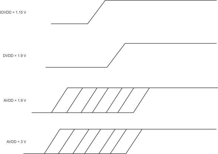
The device requires a 1.15-V nominal supply for IOVDD, a 1.9-V nominal supply for DVDD, a 1.9-V nominal supply for AVDD, and a 3.0-V nominal supply for AVDD3V. For detailed information regarding the operating voltage minimum and maximum specifications of different supplies, see the Recommended Operating Conditions table.
10.1 Power Sequencing and Initialization
Figure 138 shows the suggested power-up sequencing for the device. Note that the 1.15-V IOVDD supply must rise before the 1.9-V DVDD supply. If the 1.9-V DVDD supply rises before the 1.15-V IOVDD supply, then the internal default register settings may not load properly. The other supplies (the 3-V AVDD3V and the 1.9-V AVDD), can come up in any order during the power sequence. The power supplies can ramp up at any rate and there is no hard requirement for the time delay between IOVDD ramp up to DVDD ramp-up (can be in orders of microseconds but is recommend to be a few milliseconds).
 Figure 138. Power Sequencing for the ADS54Jxx Family of Devices