ZHCSF28B May 2016 – January 2017 ADS54J20
PRODUCTION DATA.
- 1 特性
- 2 应用
- 3 说明
- 4 修订历史记录
- 5 Device Comparison Table
- 6 Pin Configuration and Functions
- 7 Specifications
-
8 Detailed Description
- 8.1 Overview
- 8.2 Functional Block Diagram
- 8.3 Feature Description
- 8.4 Device Functional Modes
- 8.5
Register Maps
- 8.5.1 Detailed Register Information
- 8.5.2 Example Register Writes
- 8.5.3
Register Descriptions
- 8.5.3.1 General Registers
- 8.5.3.2
Master Page (080h) Registers
- 8.5.3.2.1 Register 20h (address = 20h), Master Page (080h)
- 8.5.3.2.2 Register 21h (address = 21h), Master Page (080h)
- 8.5.3.2.3 Register 23h (address = 23h), Master Page (080h)
- 8.5.3.2.4 Register 24h (address = 24h), Master Page (080h)
- 8.5.3.2.5 Register 26h (address = 26h), Master Page (080h)
- 8.5.3.2.6 Register 4Fh (address = 4Fh), Master Page (080h)
- 8.5.3.2.7 Register 53h (address = 53h), Master Page (080h)
- 8.5.3.2.8 Register 54h (address = 54h), Master Page (080h)
- 8.5.3.2.9 Register 55h (address = 55h), Master Page (080h)
- 8.5.3.2.10 Register 59h (address = 59h), Master Page (080h)
- 8.5.3.3 ADC Page (0Fh) Register
- 8.5.3.4
Main Digital Page (6800h) Registers
- 8.5.3.4.1 Register 0h (address = 0h), Main Digital Page (6800h)
- 8.5.3.4.2 Register 41h (address = 41h), Main Digital Page (6800h)
- 8.5.3.4.3 Register 42h (address = 42h), Main Digital Page (6800h)
- 8.5.3.4.4 Register 43h (address = 43h), Main Digital Page (6800h)
- 8.5.3.4.5 Register 44h (address = 44h), Main Digital Page (6800h)
- 8.5.3.4.6 Register 4Bh (address = 4Bh), Main Digital Page (6800h)
- 8.5.3.4.7 Register 4Dh (address = 4Dh), Main Digital Page (6800h)
- 8.5.3.4.8 Register 4Eh (address = 4Eh), Main Digital Page (6800h)
- 8.5.3.4.9 Register 52h (address = 52h), Main Digital Page (6800h)
- 8.5.3.4.10 Register 72h (address = 72h), Main Digital Page (6800h)
- 8.5.3.4.11 Register ABh (address = ABh), Main Digital Page (6800h)
- 8.5.3.4.12 Register ADh (address = ADh), Main Digital Page (6800h)
- 8.5.3.4.13 Register F7h (address = F7h), Main Digital Page (6800h)
- 8.5.3.5
JESD Digital Page (6900h) Registers
- 8.5.3.5.1 Register 0h (address = 0h), JESD Digital Page (6900h)
- 8.5.3.5.2 Register 1h (address = 1h), JESD Digital Page (6900h)
- 8.5.3.5.3 Register 2h (address = 2h), JESD Digital Page (6900h)
- 8.5.3.5.4 Register 3h (address = 3h), JESD Digital Page (6900h)
- 8.5.3.5.5 Register 5h (address = 5h), JESD Digital Page (6900h)
- 8.5.3.5.6 Register 6h (address = 6h), JESD Digital Page (6900h)
- 8.5.3.5.7 Register 7h (address = 7h), JESD Digital Page (6900h)
- 8.5.3.5.8 Register 16h (address = 16h), JESD Digital Page (6900h)
- 8.5.3.5.9 Register 31h (address = 31h), JESD Digital Page (6900h)
- 8.5.3.5.10 Register 32h (address = 32h), JESD Digital Page (6900h)
- 8.5.3.6
JESD Analog Page (6A00h) Registers
- 8.5.3.6.1 Registers 12h-5h (addresses = 12h-5h), JESD Analog Page (6A00h)
- 8.5.3.6.2 Register 16h (address = 16h), JESD Analog Page (6A00h)
- 8.5.3.6.3 Register 17h (address = 17h), JESD Analog Page (6A00h)
- 8.5.3.6.4 Register 1Ah (address = 1Ah), JESD Analog Page (6A00h)
- 8.5.3.6.5 Register 1Bh (address = 1Bh), JESD Analog Page (6A00h)
- 9 Application and Implementation
- 10Power Supply Recommendations
- 11Layout
- 12器件和文档支持
- 13机械、封装和可订购信息
9 Application and Implementation
NOTE
Information in the following applications sections is not part of the TI component specification, and TI does not warrant its accuracy or completeness. TI’s customers are responsible for determining suitability of components for their purposes. Customers should validate and test their design implementation to confirm system functionality.
9.1 Application Information
9.1.1 Start-Up Sequence
The steps described in Table 65 are recommended as the power-up sequence with the ADS54J20 in 20X mode (LMFS = 8224).
Table 65. Initialization Sequence
| STEP | SEQUENCE | DESCRIPTION | PAGE BEING PROGRAMMED | COMMENT |
|---|---|---|---|---|
| 1 | Power-up the device | Bring up IOVDD to 1.15 V before applying power to DVDD. Bring up DVDD to 1.9 V, AVDD to 1.9 V, and AVDD3V to 3.0 V. | — | See the Power Sequencing and Initialization section for power sequence requirements. |
| 2 | Reset the device | Hardware reset | ||
| Apply a hardware reset by pulsing pin 48 (low → high → low). | — | A hardware reset clears all registers to their default values. | ||
| Register writes are equivalent to a hardware reset. | ||||
| Write address 0-000h with 81h. | General register | Reset registers in the ADC and master pages of the analog bank. | ||
| This bit is a self-clearing bit. | ||||
| Write address 4-001h with 00h and address 4-002h with 00h. | Unused page | Clear any unwanted content from the unused pages of the JESD bank. | ||
| Write address 4-003h with 00h and address 4-004h with 68h. | — | Select the main digital page of the JESD bank. | ||
| Write address 6-0F7h with 01h for channel A. | Main digital page (JESD bank) |
Use the DIG RESET register bit to reset all pages in the JESD bank. | ||
| This bit is a self-clearing bit. | ||||
| Write address 6-000h with 01h, then address 6-000h with 00h. | Pulse the PULSE RESET register bit for channel A. | |||
| 3 | Performance modes | Write address 0-011h with 80h. | — | Select the master page of the analog bank. |
| Write address 0-059h with 20h. | Master page (analog bank) |
Set the ALWAYS WRITE 1 bit. | ||
| 4 | Program desired registers for decimation options and JESD link configuration |
Default register writes for DDC modes and JESD link configuration (LMFS = 8224). | ||
| Write address 4-003h with 00h and address 4-004h with 69h. | — | Select the JESD digital page. | ||
| Write address 6-000h with 80h. | JESD digital page (JESD bank) |
Set the CTRL K bit for both channels by programming K according to the SYSREF signal later on in the sequence. | ||
| JESD link is configured with LMFS = 8224 by default with no decimation. | See Table 14 for configuring the JESD digital page registers for the desired LMFS and programming appropriate DDC mode. | |||
| Write address 4-003h with 00h and address 4-004h with 6Ah. | — | Select the JESD analog page. | ||
| JESD link is configured with LMFS = 8224 by default with no decimation. | JESD analog page (JESD bank) |
See Table 14 for configuring the JESD analog page registers for the desired LMFS and programming appropriate DDC mode. | ||
| Write address 6-017h with 40h. | PLL reset. | |||
| Write address 6-017h with 00h. | PLL reset clear. | |||
| Write address 4-003h with 00h and address 4-004h with 68h. | — | Select the main digital page. | ||
| JESD link is configured with LMFS = 8224 by default with no decimation. | Main digital page (JESD bank) |
See Table 14 for configuring the main digital page registers for the desired LMFS and programming appropriate DDC mode. | ||
| Write address 6-000h with 01h and address 6-000h with 00h. | Pulse the PULSE RESET register bit. All settings programmed in the main digital page take effect only after this bit is pulsed. | |||
| 5 | Set the value of K and the SYSREF signal frequency accordingly | Write address 4-003h with 00h and address 4-004h with 69h. | — | Select the JESD digital page. |
| Write address 6-006h with XXh (choose the value of K). | JESD digital page (JESD bank) |
See the SYSREF Signal section to choose the correct frequency for SYSREF. | ||
| 6 | JESD lane alignment | Pull the SYNCB pin (pin 63) low. | — | Transmit K28.5 characters. |
| Pull the SYNCB pin high. | After the receiver is synchronized, initiate an ILA phase and subsequent transmissions of ADC data. | |||
9.1.2 Hardware Reset
Figure 130 and Table 66 show the timing for a hardware reset.
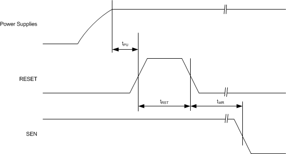 Figure 130. Hardware Reset Timing Diagram
Table 66. Timing Requirements for Figure 130
| MIN | TYP | MAX | UNIT | ||
|---|---|---|---|---|---|
| tPU | Power-on delay from power-up to an active high RESET pulse | 1 | ms | ||
| tRST | Reset pulse duration: active high RESET pulse duration | 10 | ns | ||
| tWR | Register write delay from RESET disable to SEN active | 100 | ns | ||
9.1.3 SNR and Clock Jitter
The signal-to-noise ratio (SNR) of the ADC is limited by three different factors: quantization noise, thermal noise, and jitter, as shown in Equation 4. The quantization noise is typically not noticeable in pipeline converters and is 74 dBFS for a 12-bit ADC. The thermal noise limits SNR at low input frequencies and the clock jitter sets SNR for higher input frequencies.

The SNR limitation resulting from sample clock jitter can be calculated by Equation 5:

The total clock jitter (TJitter) has two components: the internal aperture jitter (130 fS) is set by the noise of the clock input buffer and the external clock jitter. TJitter can be calculated by Equation 6:

External clock jitter can be minimized by using high-quality clock sources and jitter cleaners as well as band-pass filters at the clock input. A faster clock slew rate also improves the ADC aperture jitter.
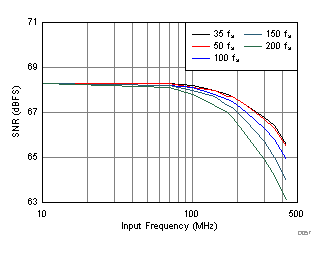
The ADS54J20 has a thermal noise of approximately 71.1 dBFS and an internal aperture jitter of 120 fS. SNR, depending on the amount of external jitter for different input frequencies, is shown in Figure 131.
9.2 Typical Application
The ADS54J20 is designed for wideband receiver applications demanding excellent dynamic range over a large input frequency range. A typical schematic for an ac-coupled receiver is shown in Figure 132.
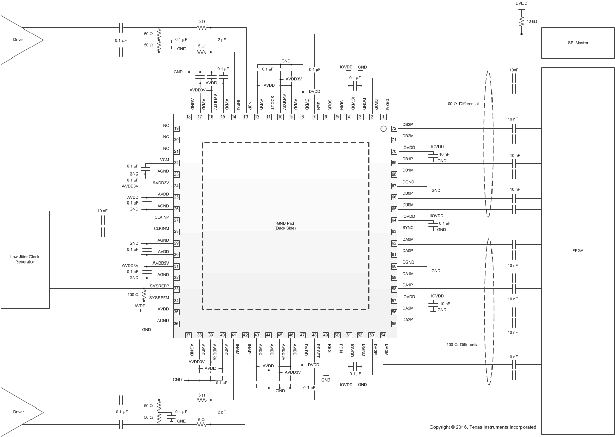
NOTE:
GND = AGND and DGND are connected in the PCB layout.9.2.1 Design Requirements
9.2.1.1 Transformer-Coupled Circuits
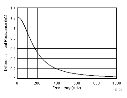
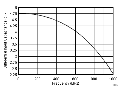
Typical applications involving transformer-coupled circuits are discussed in this section. Transformers (such as ADT1-1WT or WBC1-1) can be used up to 300 MHz to achieve good phase and amplitude balances at the ADC inputs. When designing dc-driving circuits, the ADC input impedance must be considered. Figure 133 and Figure 134 show the impedance (ZIN = RIN || CIN) across the ADC input pins.
By using the simple drive circuit of Figure 135, uniform performance can be obtained over a wide frequency range. The buffers present at the analog inputs of the device help isolate the external drive source from the switching currents of the sampling circuit.
 Figure 135. Input Drive Circuit
9.2.2 Detailed Design Procedure
For optimum performance, the analog inputs must be driven differentially. This architecture improves common-mode noise immunity and even-order harmonic rejection. A small resistor (5 Ω to 10 Ω) in series with each input pin is recommended to damp out ringing caused by package parasitics, as shown in Figure 135.
9.2.3 Application Curves
Figure 136 and Figure 137 show the typical performance at 170 MHz and 230 MHz, respectively.
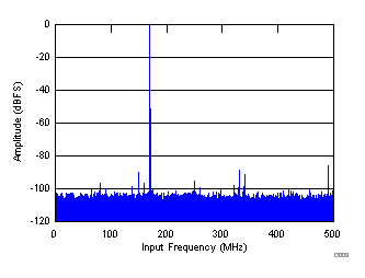
| SNR = 67.8 dBFS, SINAD = 67.7 dBFS, SFDR = 86 dBc, THD = 81 dBc, IL spur = 88 dBc, non HD2, HD3 spur = 89 dBc |
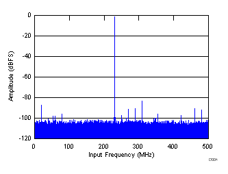
| SNR = 67.4 dBFS, SINAD = 67.2 dBFS, IL spur = 87 dBc, SFDR = 84 dBc, THD = 82 dBc, non HD2, HD3 spur = 90 dBc |