ZHCSEP7A February 2016 – March 2016 ADS54J42
PRODUCTION DATA.
- 1 特性
- 2 应用
- 3 说明
- 4 修订历史记录
- 5 Device Comparison Table
- 6 Pin Configuration and Functions
- 7 Specifications
-
8 Detailed Description
- 8.1 Overview
- 8.2 Functional Block Diagram
- 8.3 Feature Description
- 8.4 Device Functional Modes
- 8.5
Register Maps
- 8.5.1 Detailed Register Info
- 8.5.2 Example Register Writes
- 8.5.3
Register Descriptions
- 8.5.3.1 General Registers
- 8.5.3.2
Master Page (080h) Registers
- 8.5.3.2.1 Register 20h (address = 20h), Master Page (080h)
- 8.5.3.2.2 Register 21h (address = 21h), Master Page (080h)
- 8.5.3.2.3 Register 23h (address = 23h), Master Page (080h)
- 8.5.3.2.4 Register 24h (address = 24h), Master Page (080h)
- 8.5.3.2.5 Register 26h (address = 26h), Master Page (080h)
- 8.5.3.2.6 Register 39h (address = 39h), Master Page (080h)
- 8.5.3.2.7 Register 3Ah (address = 3Ah), Master Page (080h)
- 8.5.3.2.8 Register 4Fh (address = 4Fh), Master Page (080h)
- 8.5.3.2.9 Register 53h (address = 53h), Master Page (080h)
- 8.5.3.2.10 Register 55h (address = 55h), Master Page (080h)
- 8.5.3.2.11 Register 56h (address = 56h), Master Page (080h)
- 8.5.3.2.12 Register 59h (address = 59h), Master Page (080h)
- 8.5.3.3 ADC Page (0Fh) Register
- 8.5.3.4
Main Digital Page (6800h) Registers
- 8.5.3.4.1 Register 0h (address = 0h), Main Digital Page (6800h)
- 8.5.3.4.2 Register 41h (address = 41h), Main Digital Page (6800h)
- 8.5.3.4.3 Register 42h (address = 42h), Main Digital Page (6800h)
- 8.5.3.4.4 Register 43h (address = 43h), Main Digital Page (6800h)
- 8.5.3.4.5 Register 44h (address = 44h), Main Digital Page (6800h)
- 8.5.3.4.6 Register 4Bh (address = 4Bh), Main Digital Page (6800h)
- 8.5.3.4.7 Register 4Dh (address = 4Dh), Main Digital Page (6800h)
- 8.5.3.4.8 Register 4Eh (address = 4Eh), Main Digital Page (6800h)
- 8.5.3.4.9 Register 52h (address = 52h), Main Digital Page (6800h)
- 8.5.3.4.10 Register 72h (address = 72h), Main Digital Page (6800h)
- 8.5.3.4.11 Register ABh (address = ABh), Main Digital Page (6800h)
- 8.5.3.4.12 Register ADh (address = ADh), Main Digital Page (6800h)
- 8.5.3.4.13 Register F7h (address = F7h), Main Digital Page (6800h)
- 8.5.3.5
JESD Digital Page (6900h) Registers
- 8.5.3.5.1 Register 0h (address = 0h), JESD Digital Page (6900h)
- 8.5.3.5.2 Register 1h (address = 1h), JESD Digital Page (6900h)
- 8.5.3.5.3 Register 2h (address = 2h), JESD Digital Page (6900h)
- 8.5.3.5.4 Register 3h (address = 3h), JESD Digital Page (6900h)
- 8.5.3.5.5 Register 5h (address = 5h), JESD Digital Page (6900h)
- 8.5.3.5.6 Register 6h (address = 6h), JESD Digital Page (6900h)
- 8.5.3.5.7 Register 7h (address = 7h), JESD Digital Page (6900h)
- 8.5.3.5.8 Register 16h (address = 16h), JESD Digital Page (6900h)
- 8.5.3.5.9 Register 31h (address = 31h), JESD Digital Page (6900h)
- 8.5.3.5.10 Register 32h (address = 32h), JESD Digital Page (6900h)
- 8.5.3.6
JESD Analog Page (6A00h) Registers
- 8.5.3.6.1 Registers 12h-5h (addresses = 12h-5h), JESD Analog Page (6A00h)
- 8.5.3.6.2 Register 16h (address = 16h), JESD Analog Page (6A00h)
- 8.5.3.6.3 Register 17h (address = 17h), JESD Analog Page (6A00h)
- 8.5.3.6.4 Register 1Ah (address = 1Ah), JESD Analog Page (6A00h)
- 8.5.3.6.5 Register 1Bh (address = 1Bh), JESD Analog Page (6A00h)
- 9 Application and Implementation
- 10Power Supply Recommendations
- 11Layout
- 12器件和文档支持
- 13机械、封装和可订购信息
7 Specifications
7.1 Absolute Maximum Ratings
over operating free-air temperature range (unless otherwise noted)(1)| MIN | MAX | UNIT | ||
|---|---|---|---|---|
| Supply voltage range | AVDD3V | –0.3 | 3.6 | V |
| AVDD | –0.3 | 2.1 | ||
| DVDD | –0.3 | 2.1 | ||
| IOVDD | –0.2 | 1.4 | ||
| Voltage between AGND and DGND | –0.3 | 0.3 | V | |
| Voltage applied to input pins | INAP, INBP, INAM, INBM | –0.3 | 3 | V |
| CLKINP, CLKINM | –0.3 | AVDD + 0.3 | ||
| SYSREFP, SYSREFM | –0.3 | AVDD + 0.3 | ||
| SCLK, SEN, SDIN, RESET, SYNC, PDN | –0.2 | 2.1 | ||
| Storage temperature, Tstg | –65 | 150 | °C | |
(1) Stresses beyond those listed under Absolute Maximum Ratings may cause permanent damage to the device. These are stress ratings only, which do not imply functional operation of the device at these or any other conditions beyond those indicated under Recommended Operating Conditions. Exposure to absolute-maximum-rated conditions for extended periods may affect device reliability.
7.2 ESD Ratings
| VALUE | UNIT | |||
|---|---|---|---|---|
| V(ESD) | Electrostatic discharge | Human-body model (HBM), per ANSI/ESDA/JEDEC JS-001(1) | ±1000 | V |
| Charged-device model (CDM), per JEDEC specification JESD22-C101(2) | ±500 | |||
(1) JEDEC document JEP155 states that 500-V HBM allows safe manufacturing with a standard ESD control process.
(2) JEDEC document JEP157 states that 250-V HBM allows safe manufacturing with a standard ESD control process.
7.3 Recommended Operating Conditions
over operating free-air temperature range (unless otherwise noted)(2)(3)| MIN | NOM | MAX | UNIT | |||
|---|---|---|---|---|---|---|
| Supply voltage range | AVDD3V | 2.85 | 3.0 | 3.6 | V | |
| AVDD | 1.8 | 1.9 | 2.0 | |||
| DVDD | 1.7 | 1.9 | 2.0 | |||
| IOVDD | 1.1 | 1.15 | 1.2 | |||
| Analog inputs | Differential input voltage range | 1.9 | VPP | |||
| Input common-mode voltage | 2.0 | V | ||||
| Maximum analog input frequency for a 1.9-VPP input amplitude(4)(5) | 400 | MHz | ||||
| Clock inputs | Input clock frequency, device clock frequency | 300(6) | 625 | MHz | ||
| Input clock amplitude differential (VCLKP – VCLKM) |
Sine wave, ac-coupled | 0.75 | 1.5 | VPP | ||
| LVPECL, ac-coupled | 0.8 | 1.6 | ||||
| LVDS, ac-coupled | 0.7 | |||||
| Input device clock duty cycle | 45% | 50% | 55% | |||
| Temperature | Operating free-air, TA | –40 | 85 | ºC | ||
| Operating junction, TJ | 105(1) | 125 | ||||
(1) Prolonged use above the nominal junction temperature can increase the device failure-in-time (FIT) rate.
(2) SYSREF must be applied for the device to initialize; see the SYSREF Signal section for details.
(3) After power-up, always use a hardware reset to reset the device for the first time; see Table 66 for details.
(4) Operating 0.5 dB below the maximum-supported amplitude is recommended to accommodate gain mismatch in interleaving ADCs.
(5) At high frequencies, the maximum supported input amplitude reduces; see Figure 36 for details.
(6) See Table 9.
7.4 Thermal Information
| THERMAL METRIC(1) | ADS54J42 | UNIT | |
|---|---|---|---|
| RMP (VQFNP) | |||
| 72 PINS | |||
| RθJA | Junction-to-ambient thermal resistance | 22.3 | °C/W |
| RθJC(top) | Junction-to-case (top) thermal resistance | 5.1 | °C/W |
| RθJB | Junction-to-board thermal resistance | 2.4 | °C/W |
| ψJT | Junction-to-top characterization parameter | 0.1 | °C/W |
| ψJB | Junction-to-board characterization parameter | 2.3 | °C/W |
| RθJC(bot) | Junction-to-case (bottom) thermal resistance | 0.4 | °C/W |
(1) For more information about traditional and new thermal metrics, see the IC Package Thermal Metrics application report, SPRA953.
7.5 Electrical Characteristics
typical values are at TA = 25°C, full temperature range is from TMIN = –40°C to TMAX = 85°C, ADC sampling rate = 625 MSPS, 50% clock duty cycle, AVDD3V = 3.0 V, AVDD = DVDD = 1.9 V, IOVDD = 1.15 V, and –1-dBFS differential input (unless otherwise noted)| PARAMETER | TEST CONDITIONS | MIN | TYP | MAX | UNIT | ||
|---|---|---|---|---|---|---|---|
| GENERAL | |||||||
| ADC sampling rate | 625 | MSPS | |||||
| Resolution | 14 | Bits | |||||
| POWER SUPPLIES | |||||||
| AVDD3V | 3.0-V analog supply | 2.85 | 3.0 | 3.6 | V | ||
| AVDD | 1.9-V analog supply | 1.8 | 1.9 | 2.0 | V | ||
| DVDD | 1.9-V digital supply | 1.7 | 1.9 | 2.0 | V | ||
| IOVDD | 1.15-V SERDES supply | 1.1 | 1.15 | 1.2 | V | ||
| IAVDD3V | 3.0-V analog supply current | VIN = full-scale on both channels | 247 | 310 | mA | ||
| IAVDD | 1.9-V analog supply current | VIN = full-scale on both channels | 260 | 410 | mA | ||
| IDVDD | 1.9-V digital supply current | Eight lanes active (LMFS = 8224) |
137 | 210 | mA | ||
| IIOVDD | 1.15-V SERDES supply current | Eight lanes active (LMFS = 8224) |
382 | 720 | mA | ||
| Pdis | Total power dissipation | Eight lanes active (LMFS = 8224) |
1.94 | 2.68 | W | ||
| IDVDD | 1.9-V digital supply current | Four lanes active (LMFS = 4222), 2X decimation | 130 | mA | |||
| IIOVDD | 1.15-V SERDES supply current | Four lanes active (LMFS = 4222), 2X decimation | 404 | mA | |||
| Pdis | Total power dissipation | Four lanes active (LMFS = 4222), 2X decimation | 1.95 | W | |||
| IDVDD | 1.9-V digital supply current | Two lanes active (LMFS = 2221), 4X decimation | 129 | mA | |||
| IIOVDD | 1.15-V SERDES supply current | Two lanes active (LMFS = 2221), 4X decimation | 400 | mA | |||
| Pdis(1) | Total power dissipation | Two lanes active (LMFS = 2221), 4X decimation | 1.94 | W | |||
| Global power-down power dissipation | 285 | 315 | mW | ||||
| ANALOG INPUTS (INAP, INAM, INBP, INBM) | |||||||
| Differential input full-scale voltage | 1.9 | VPP | |||||
| VIC | Common-mode input voltage | 2.0 | V | ||||
| RIN | Differential input resistance | At 170-MHz input frequency | 0.6 | kΩ | |||
| CIN | Differential input capacitance | At 170-MHz input frequency | 4.7 | pF | |||
| Analog input bandwidth (3 dB) | 50-Ω source driving ADC inputs terminated with 50 Ω | 1.2 | GHz | ||||
| CLOCK INPUT (CLKINP, CLKINM) | |||||||
| Internal clock biasing | CLKINP and CLKINM are connected to internal biasing voltage through 400 Ω | 1.15 | V | ||||
(1) See the Power-Down Mode section for details.
7.6 AC Characteristics
typical values are at TA = 25°C, full temperature range is from TMIN = –40°C to TMAX = 85°C, ADC sampling rate = 625 MSPS, 50% clock duty cycle, AVDD3V = 3.0 V, AVDD = DVDD = 1.9 V, IOVDD = 1.15 V, –1-dBFS differential input amplitude, and 0-dB digital gain (unless otherwise noted)7.7 Digital Characteristics
typical values are at TA = 25°C, full temperature range is from TMIN = –40°C to TMAX = 85°C, ADC sampling rate = 625 MSPS, 50% clock duty cycle, AVDD3V = 3.0 V, AVDD = DVDD = 1.9 V, IOVDD = 1.15 V, and –1-dBFS differential input (unless otherwise noted)| PARAMETER | TEST CONDITIONS | MIN | TYP | MAX | UNITS | |
|---|---|---|---|---|---|---|
| DIGITAL INPUTS (RESET, SCLK, SEN, SDIN, SYNC, PDN)(1) | ||||||
| VIH | High-level input voltage | All digital inputs support 1.2-V and 1.8-V logic levels | 0.8 | V | ||
| VIL | Low-level input voltage | All digital inputs support 1.2-V and 1.8-V logic levels | 0.4 | V | ||
| IIH | High-level input current | SEN | 0 | µA | ||
| RESET, SCLK, SDIN, PDN, SYNC | 50 | |||||
| IIL | Low-level input current | SEN | 50 | µA | ||
| RESET, SCLK, SDIN, PDN, SYNC | 0 | |||||
| DIGITAL INPUTS (SYSREFP, SYSREFM) | ||||||
| VD | Differential input voltage | 0.35 | 0.45 | 1.4 | V | |
| V(CM_DIG) | Common-mode voltage for SYSREF(3) | 1.3 | V | |||
| DIGITAL OUTPUTS (SDOUT, PDN(3)) | ||||||
| VOH | High-level output voltage | DVDD – 0.1 | DVDD | V | ||
| VOL | Low-level output voltage | 0.1 | V | |||
| DIGITAL OUTPUTS (JESD204B Interface: DxP, DxM)(2) | ||||||
| VOD | Output differential voltage | With default swing setting | 700 | mVPP | ||
| VOC | Output common-mode voltage | 450 | mV | |||
| Transmitter short-circuit current | Transmitter pins shorted to any voltage between –0.25 V and 1.45 V | –100 | 100 | mA | ||
| zos | Single-ended output impedance | 50 | Ω | |||
| Output capacitance | Output capacitance inside the device, from either output to ground |
2 | pF | |||
(1) The RESET, SCLK, SDIN, and PDN pins have a 20-kΩ (typical) internal pulldown resistor to ground, and the SEN pin has a 20-kΩ (typical) pullup resistor to IOVDD.
(2) 100-Ω differential termination.
(3) When functioning as an OVR pin for channel B.
7.8 Timing Characteristics
typical values are at TA = 25°C, full temperature range is from TMIN = –40°C to TMAX = 85°C, ADC sampling rate = 625 MSPS, 50% clock duty cycle, AVDD3V = 3.0 V, AVDD = DVDD = 1.9 V, IOVDD = 1.15 V, and –1-dBFS differential input (unless otherwise noted)| MIN | TYP | MAX | UNITS | |||
|---|---|---|---|---|---|---|
| SAMPLE TIMING | ||||||
| Aperture delay | 0.75 | 1.6 | ns | |||
| Aperture delay matching between two channels on the same device | ±70 | ps | ||||
| Aperture delay matching between two devices at the same temperature and supply voltage | ±270 | ps | ||||
| Aperture jitter | 120 | fS rms | ||||
| WAKE-UP TIMING | ||||||
| Wake-up time to valid data after coming out of global power-down | 150 | µs | ||||
| LATENCY | ||||||
| Data latency(1): ADC sample to digital output | 134 | Input clock cycles | ||||
| OVR latency: ADC sample to OVR bit | 62 | Input clock cycles | ||||
| tPD | Propagation delay: logic gates and output buffers delay (does not change with fS) | 4 | ns | |||
| SYSREF TIMING | ||||||
| tSU_SYSREF | Setup time for SYSREF, referenced to the input clock falling edge | 300 | 900 | ps | ||
| tH_SYSREF | Hold time for SYSREF, referenced to the input clock falling edge | 100 | ps | |||
| JESD OUTPUT INTERFACE TIMING CHARACTERISTICS | ||||||
| Unit interval | 160 | 400 | ps | |||
| Serial output data rate | 2.5 | 6.25 | Gbps | |||
| Total jitter for BER of 1E-15 and lane rate = 6.25 Gbps | 26 | ps | ||||
| Random jitter for BER of 1E-15 and lane rate = 6.25 Gbps | 0.75 | ps rms | ||||
| Deterministic jitter for BER of 1E-15 and lane rate = 6.25 Gbps | 12 | ps, pk-pk | ||||
| tR, tF | Data rise time, data fall time: rise and fall times are measured from 20% to 80%, differential output waveform, 2.5 Gbps ≤ bit rate ≤ 6.25 Gbps |
35 | ps | |||
(1) Overall ADC latency = data latency + tPDI.
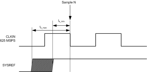 Figure 1. SYSREF Timing
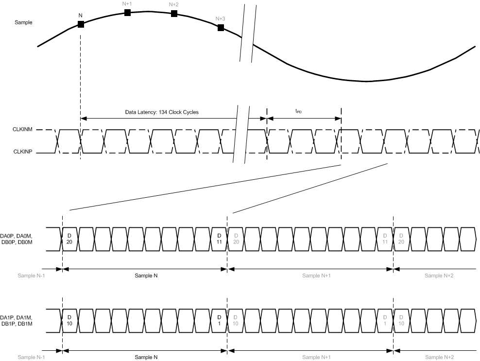 Figure 2. Sample Timing Requirements
7.9 Typical Characteristics
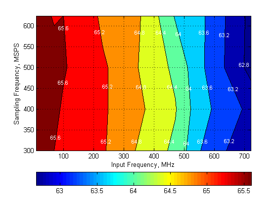
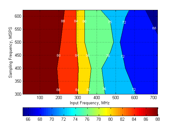
typical values are at TA = 25°C, full temperature range is from TMIN = –40°C to TMAX = 85°C, ADC sampling rate = 625 MSPS, 50% clock duty cycle, AVDD3V = 3.0 V, AVDD = DVDD = 1.9 V, IOVDD = 1.15 V, –1-dBFS differential input, and 0-dB digital gain (unless otherwise noted)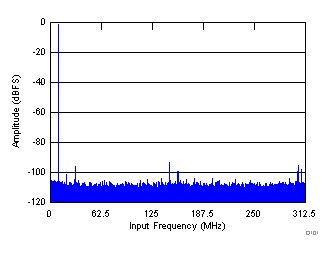
| SNR = 71.9 dBFS, SINAD = 71.86 dBFS, THD = 93 dBc, IL spur = 94 dBc, SFDR = 94 dBc, non HD2, HD3 spur = 94 dBc |
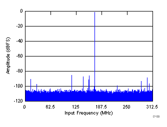
| SNR = 71 dBFS, SINAD = 70.9 dBFS, SFDR = 85 dBc, THD = 84 dBc, IL spur = 87 dBc, non HD2, HD3 spur = 93 dBc |
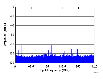
| SNR = 69.5 dBFS, SINAD = 69.1 dBFS, IL spur = 81 dBc, SFDR = 80 dBc, THD = 79 dBc, non HD2, HD3 spur = 90 dBc |
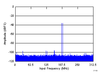
| fIN1 = 185 MHz, fIN2 = 190 MHz, each tone at –36 dBFS, IMD = 107 dBFS |
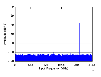
| fIN1 = 370 MHz, fIN2 = 365 MHz, each tone at –36 dBFS, IMD = 109 dBFS |
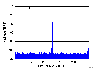
| fIN1 = 470 MHz, fIN2 = 465 MHz, each tone at –36 dBFS, IMD = 107 dBFS |
(–36 dBFS)
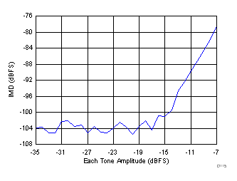
| fIN1 = 365 MHz, fIN2 = 370 MHz |
(365 MHz and 370 MHz)
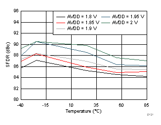
| fIN = 170 MHz |
AVDD Supply and Temperature
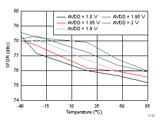
| fIN = 350 MHz |
AVDD Supply and Temperature
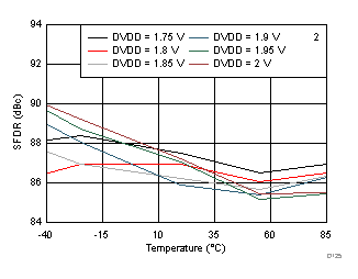
| fIN = 170 MHz |
DVDD Supply and Temperature
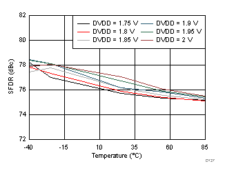
| fIN = 350 MHz |
DVDD Supply and Temperature
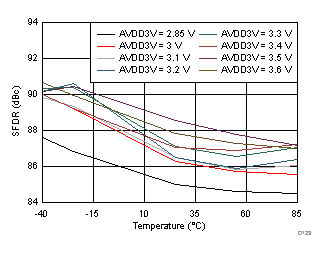
| fIN = 170 MHz |
AVDD3V Supply and Temperature
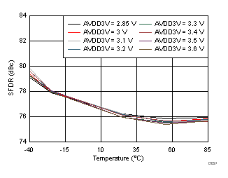
| fIN = 350 MHz |
AVDD3V Supply and Temperature
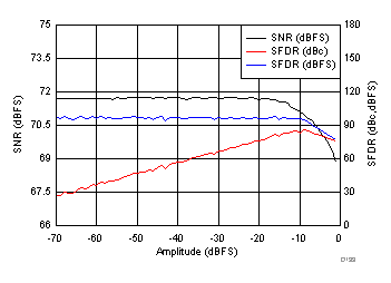
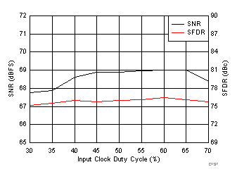
| fIN = 350 MHz |
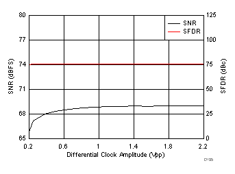
| fIN = 350 MHz |
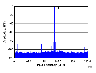
| fIN = 350 MHz |
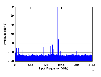
| fIN = 170 MHz, AIN = –1 dBFS, fPSRR = 5 MHz, APSRR= 50 mVPP, PSRR (AVDD supply) = 51 dB |
for Test Signal on the AVDD Supply
| fIN = 170 MHz, AIN = –1 dBFS, fCMRR = 5 MHz, ACMRR= 50 mVPP, CMRR = 40 dB |
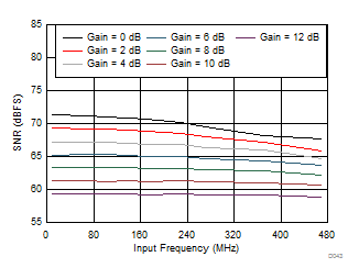
Gain and Input Frequency
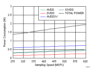
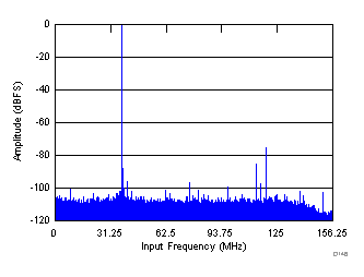
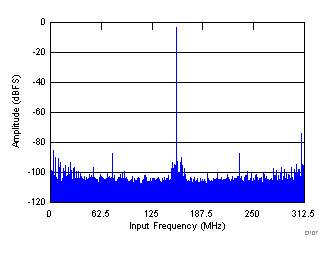
| SNR = 72 dBFS, SINAD = 71.8 dBFS, SFDR = 84 dBc, THD = 83 dBc, non HD2, HD3 spur = 98 dBc |
Decimate-by-2 Mode
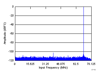
| SNR = 77.4 dBFS, SINAD = 77.3 dBFS, SFDR = 105 dBc, THD = 102 dBc, non HD2, HD3 spur = 105 dBc |
Decimate-by-4 Mode
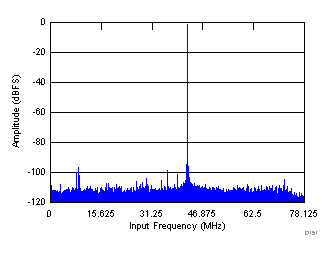
| SNR = 74.9 dBFS, SINAD = 74.8 dBFS, SFDR = 93 dBc, THD = 92 dBc, non HD2, HD3 spur = 93 dBc |
Decimate-by-4 Mode
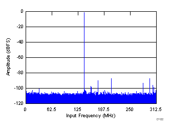
| SNR = 71.3 dBFS, SINAD = 71.1 dBFS, SFDR = 86 dBc, THD = 85 dBc, IL spur = 87 dBc, non HD2, HD3 spur = 95 dBc |
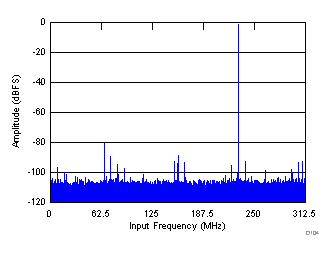
| SNR = 70.4 dBFS, SINAD = 69.9 dBFS, IL spur = 89 dBc, SFDR = 80 dBc, THD = 79 dBc, non HD2, HD3 spur = 91 dBc |
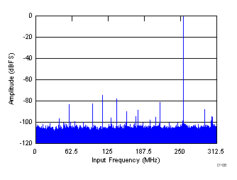
| SNR = 68.8 dBFS, SINAD = 67.3 dBFS, SFDR = 73 dBc, THD = 72 dBc, IL spur = 81 dBc, non HD2, HD3 spur = 89 dBc |
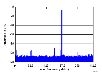
| fIN1 = 185 MHz, fIN2 = 190 MHz, each tone at –7 dBFS, IMD = 89 dBFS |
||
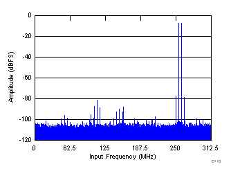
| fIN1 = 370 MHz, fIN2 = 365 MHz, each tone at –7 dBFS, IMD = 78 dBFS |
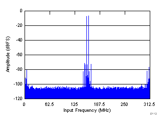
| fIN1 = 470 MHz, fIN2 = 465 MHz, each tone at –7 dBFS, IMD = 71 dBFS |
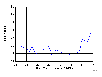
| fIN1 = 185 MHz, fIN2 = 190 MHz | ||
(185 MHz and 190 MHz)
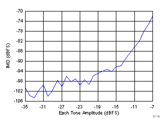
| fIN1 = 465 MHz, fIN2 = 470 MHz |
(465 MHz and 470 MHz)
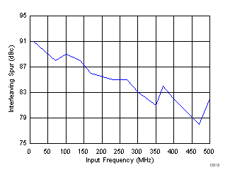
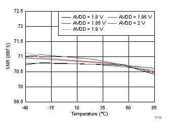
| fIN = 170 MHz |
AVDD Supply and Temperature
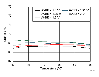
| fIN = 350 MHz |
AVDD Supply and Temperature
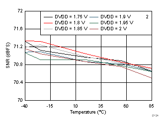
| fIN = 170 MHz |
DVDD Supply and Temperature
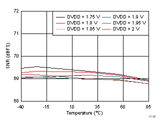
| fIN = 350 MHz |
DVDD Supply and Temperature
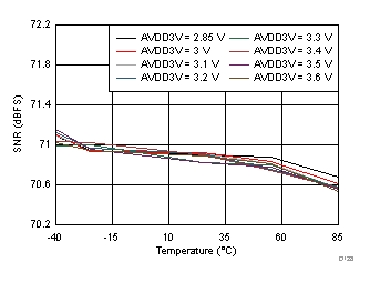
| fIN = 170 MHz |
AVDD3V Supply and Temperature
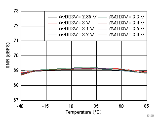
| fIN = 350 MHz |
AVDD3V Supply and Temperature
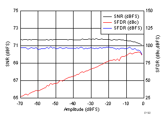
| fIN = 170 MHz |
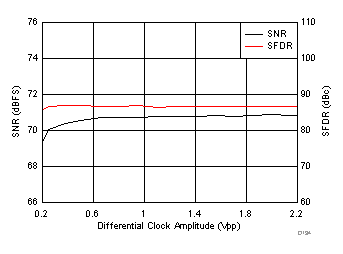
| fIN = 170 MHz |
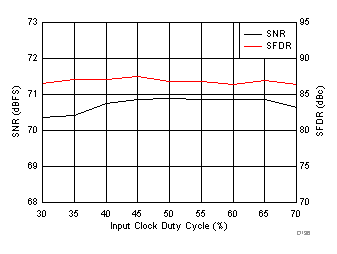
| fIN = 170 MHz |
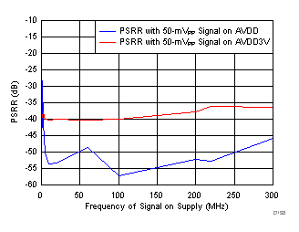
Test Signal on AVDD
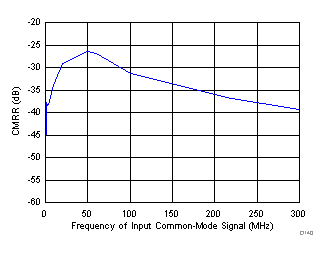
Common-Mode Signal
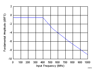
Input Frequency
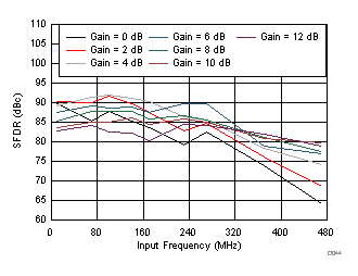
| NOTE: ADC output amplitude is –1 dBFS, input amplitude is scaled down by the amount of programmed digital gain. |
Gain and Input Frequency
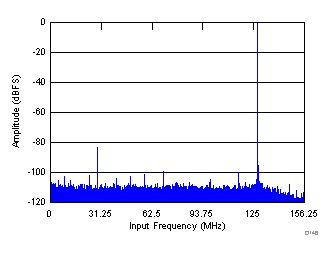
| SNR = 74.1 dBFS, SINAD = 74.09 dBFS, SFDR = 98 dBc, THD = 93 dBc, non HD2, HD3 spur = 99 dBc |
Decimate-by-2 Mode
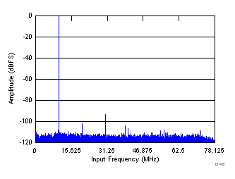
| SNR = 77.6 dBFS, SINAD = 77.5 dBFS, SFDR = 93 dBc, THD = 92 dBc, non HD2, HD3 spur = 106 dBc |
Decimate-by-4 Mode
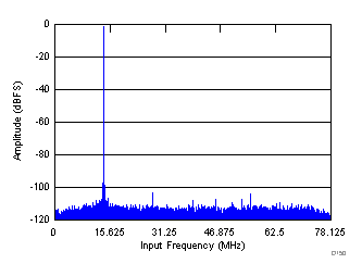
| SNR = 76.7 dBFS, SINAD = 76.6 dBFS, SFDR = 96 dBc, THD = 98 dBc, non HD2, HD3 spur = 96 dBc |
Decimate-by-4 Mode
