ZHCSE42D April 2015 – April 2019 ADS54J60
PRODUCTION DATA.
- 1 特性
- 2 应用
- 3 说明
- 4 修订历史记录
- 5 Device Comparison Table
- 6 Pin Configuration and Functions
- 7 Specifications
-
8 Detailed Description
- 8.1 Overview
- 8.2 Functional Block Diagram
- 8.3 Feature Description
- 8.4 Device Functional Modes
- 8.5
Register Maps
- 8.5.1 Example Register Writes
- 8.5.2
Register Descriptions
- 8.5.2.1 General Registers
- 8.5.2.2
Master Page (080h) Registers
- 8.5.2.2.1 Register 20h (address = 20h), Master Page (080h)
- 8.5.2.2.2 Register 21h (address = 21h), Master Page (080h)
- 8.5.2.2.3 Register 23h (address = 23h), Master Page (080h)
- 8.5.2.2.4 Register 24h (address = 24h), Master Page (080h)
- 8.5.2.2.5 Register 26h (address = 26h), Master Page (080h)
- 8.5.2.2.6 Register 4Fh (address = 4Fh), Master Page (080h)
- 8.5.2.2.7 Register 53h (address = 53h), Master Page (080h)
- 8.5.2.2.8 Register 54h (address = 54h), Master Page (080h)
- 8.5.2.2.9 Register 55h (address = 55h), Master Page (080h)
- 8.5.2.2.10 Register 59h (address = 59h), Master Page (080h)
- 8.5.2.3 ADC Page (0Fh) Register
- 8.5.2.4
Main Digital Page (6800h) Registers
- 8.5.2.4.1 Register 0h (address = 0h), Main Digital Page (6800h)
- 8.5.2.4.2 Register 41h (address = 41h), Main Digital Page (6800h)
- 8.5.2.4.3 Register 42h (address = 42h), Main Digital Page (6800h)
- 8.5.2.4.4 Register 43h (address = 43h), Main Digital Page (6800h)
- 8.5.2.4.5 Register 44h (address = 44h), Main Digital Page (6800h)
- 8.5.2.4.6 Register 4Bh (address = 4Bh), Main Digital Page (6800h)
- 8.5.2.4.7 Register 4Dh (address = 4Dh), Main Digital Page (6800h)
- 8.5.2.4.8 Register 4Eh (address = 4Eh), Main Digital Page (6800h)
- 8.5.2.4.9 Register 52h (address = 52h), Main Digital Page (6800h)
- 8.5.2.4.10 Register 72h (address = 72h), Main Digital Page (6800h)
- 8.5.2.4.11 Register ABh (address = ABh), Main Digital Page (6800h)
- 8.5.2.4.12 Register ADh (address = ADh), Main Digital Page (6800h)
- 8.5.2.4.13 Register F7h (address = F7h), Main Digital Page (6800h)
- 8.5.2.5
JESD Digital Page (6900h) Registers
- 8.5.2.5.1 Register 0h (address = 0h), JESD Digital Page (6900h)
- 8.5.2.5.2 Register 1h (address = 1h), JESD Digital Page (6900h)
- 8.5.2.5.3 Register 2h (address = 2h), JESD Digital Page (6900h)
- 8.5.2.5.4 Register 3h (address = 3h), JESD Digital Page (6900h)
- 8.5.2.5.5 Register 5h (address = 5h), JESD Digital Page (6900h)
- 8.5.2.5.6 Register 6h (address = 6h), JESD Digital Page (6900h)
- 8.5.2.5.7 Register 7h (address = 7h), JESD Digital Page (6900h)
- 8.5.2.5.8 Register 16h (address = 16h), JESD Digital Page (6900h)
- 8.5.2.5.9 Register 31h (address = 31h), JESD Digital Page (6900h)
- 8.5.2.5.10 Register 32h (address = 32h), JESD Digital Page (6900h)
- 8.5.2.6
JESD Analog Page (6A00h) Registers
- 8.5.2.6.1 Register 12h (address = 12h), JESD Analog Page (6A00h)
- 8.5.2.6.2 Registers 13h-15h (address = 13h-15h), JESD Analog Page (6A00h)
- 8.5.2.6.3 Register 16h (address = 16h), JESD Analog Page (6A00h)
- 8.5.2.6.4 Register 17h (address = 17h), JESD Analog Page (6A00h)
- 8.5.2.6.5 Register 1Ah (address = 1Ah), JESD Analog Page (6A00h)
- 8.5.2.6.6 Register 1Bh (address = 1Bh), JESD Analog Page (6A00h)
- 8.5.2.7
Offset Read Page (JESD BANK PAGE SEL = 6100h, JESD BANK PAGE SEL1 = 0000h) Registers
- 8.5.2.7.1 Register 068h (address = 068h), Offset Read Page
- 8.5.2.7.2 Register 069h (address = 069h), Offset Read Page
- 8.5.2.7.3 Registers 074h, 076h, 078h, 7Ah (address = 074h, 076h, 078h, 7Ah), Offset Read Page
- 8.5.2.7.4 Registers 075h, 077h, 079h, 7Bh (address = 075h, 077h, 079h, 7Bh), Offset Read Page
- 8.5.2.8 Offset Load Page (JESD BANK PAGE SEL= 6100h, JESD BANK PAGE SEL1 = 0500h) Registers
- 9 Application and Implementation
- 10Power Supply Recommendations
- 11Layout
- 12器件和文档支持
- 13机械、封装和可订购信息
9.1.4 DC Offset Correction Block in the ADS54J60
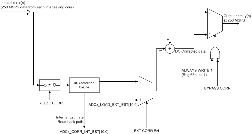
The ADS54J60 employs eight dc offset correction blocks (four per channel, one per interleaving core). Figure 142 shows a dc correction block diagram.
 Figure 142. DC Offset Correction Block Diagram
 The purpose of the dc offset correction block is to correct the dc offset of interleaving cores that mainly arise from the amplifier in the first pipeline stage. Any mismatch in dc offset among interleaving cores results in spurs at fS / 4 and fS / 2. The dc offset correction blocks estimate and correct the dc offset of an individual core, to the ideal mid-code value, and thereby remove the effect of offset mismatch.
The dc offset correction block can correct the dc offset of an individual core up to ±1024 codes.
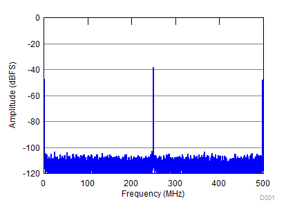
In applications involving dc-coupling between the ADC and the driver, the dc offset correction block can either be bypassed or frozen because the block cannot distinguish the external dc signal from the internal dc offset. Figure 143 shows that when bypassed, the internal dc mismatch appears at dc, fS / 4, and fS / 2 frequency points and can be as big as –40 dBFS.
 Figure 143. FFT After Bypassing the DC Offset Correction Block