ZHCSGX5 October 2017 ADS54J64
PRODUCTION DATA.
- 1 特性
- 2 应用
- 3 说明
- 4 修订历史记录
- 5 Pin Configuration and Functions
-
6 Specifications
- 6.1 Absolute Maximum Ratings
- 6.2 ESD Ratings
- 6.3 Recommended Operating Conditions
- 6.4 Thermal Information
- 6.5 Electrical Characteristics
- 6.6 AC Performance
- 6.7 Digital Characteristics
- 6.8 Timing Characteristics
- 6.9 Typical Characteristics: DDC Bypass Mode
- 6.10 Typical Characteristics: Mode 2
- 6.11 Typical Characteristics: Mode 0
- 6.12 Typical Characteristics: Dual ADC Mode
-
7 Detailed Description
- 7.1 Overview
- 7.2 Functional Block Diagram
- 7.3 Feature Description
- 7.4
Device Functional Modes
- 7.4.1
Digital Functions
- 7.4.1.1 Numerically Controlled Oscillators (NCOs) and Mixers
- 7.4.1.2 Decimation Filter
- 7.4.1.3 Mode 0: Decimate-by-4 With IQ Outputs and fS / 4 Mixer
- 7.4.1.4 Mode 1: Decimate-by-4 With IQ Outputs and 16-Bit NCO
- 7.4.1.5 Mode 2: Decimate-by-4 With Real Output
- 7.4.1.6 Mode 3: Decimate-by-2 Real Output With Frequency Shift
- 7.4.1.7 Mode 4: Decimate-by-4 With Real Output
- 7.4.1.8 Mode 6: Decimate-by-4 With IQ Outputs for Up to 110 MHz of IQ Bandwidth
- 7.4.1.9 Mode 7: Decimate-by-4 With Real Output and Zero Stuffing
- 7.4.1.10 Mode 8: DDC Bypass Mode
- 7.4.1.11 Averaging Mode
- 7.4.1.12 Overrange Indication
- 7.4.1
Digital Functions
- 7.5 Programming
- 7.6
Register Maps
- 7.6.1
Register Map
- 7.6.1.1
Register Description
- 7.6.1.1.1
GLOBAL Page Register Description
- 7.6.1.1.1.1 Register 00h (address = 00h) [reset = 0h], GLOBAL Page
- 7.6.1.1.1.2 Register 04h (address = 04h) [reset = 0h], GLOBAL Page
- 7.6.1.1.1.3 Register 11h (address = 11h) [reset = 0h], GLOBAL Page
- 7.6.1.1.1.4 Register 12h (address = 12h) [reset = 0h], GLOBAL Page
- 7.6.1.1.1.5 Register 13h (address = 13h) [reset = 0h], GLOBAL Page
- 7.6.1.1.2
DIGTOP Page Register Description
- 7.6.1.1.2.1 Register 64h (address = 64h) [reset = 0h], DIGTOP Page
- 7.6.1.1.2.2 Register 8Dh (address = 8Dh) [reset = 0h], DIGTOP Page
- 7.6.1.1.2.3 Register 8Eh (address = 8Eh) [reset = 0h], DIGTOP Page
- 7.6.1.1.2.4 Register 8Fh (address = 8Fh) [reset = 0h], DIGTOP Page
- 7.6.1.1.2.5 Register 90h (address = 90h) [reset = 0h], DIGTOP Page
- 7.6.1.1.2.6 Register 91h (address = 91h) [reset = 0h], DIGTOP Page
- 7.6.1.1.2.7 Register A5h (address = A5h) [reset = 0h], DIGTOP Page
- 7.6.1.1.2.8 Register A6h (address = A6h) [reset = 0h], DIGTOP Page
- 7.6.1.1.2.9 Register ABh (address = ABh) [reset = 0h], DIGTOP Page
- 7.6.1.1.2.10 Register ACh (address = ACh) [reset = 0h], DIGTOP Page
- 7.6.1.1.2.11 Register ADh (address = ADh) [reset = 0h], DIGTOP Page
- 7.6.1.1.2.12 Register AEh (address = AEh) [reset = 0h], DIGTOP Page
- 7.6.1.1.2.13 Register B7h (address = B7h) [reset = 0h], DIGTOP Page
- 7.6.1.1.2.14 Register 8Ch (address = 8Ch) [reset = 0h], DIGTOP Page
- 7.6.1.1.3
ANALOG Page Register Description
- 7.6.1.1.3.1 Register 6Ah (address = 6Ah) [reset = 0h], ANALOG Page
- 7.6.1.1.3.2 Register 6Fh (address = 6Fh) [reset = 0h], ANALOG Page
- 7.6.1.1.3.3 Register 71h (address = 71h) [reset = 0h], ANALOG Page
- 7.6.1.1.3.4 Register 72h (address = 72h) [reset = 0h], ANALOG Page
- 7.6.1.1.3.5 Register 93h (address = 93h) [reset = 0h], ANALOG Page
- 7.6.1.1.3.6 Register 94h (address = 94h) [reset = 0h], ANALOG Page
- 7.6.1.1.3.7 Register 9Bh (address = 9Bh) [reset = 0h], ANALOG Page
- 7.6.1.1.3.8 Register 9Dh (address = 9Dh) [reset = 0h], ANALOG Page
- 7.6.1.1.3.9 Register 9Eh (address = 9Eh) [reset = 0h], ANALOG Page
- 7.6.1.1.3.10 Register 9Fh (address = 9Fh) [reset = 0h], ANALOG Page
- 7.6.1.1.3.11 Register AFh (address = AFh) [reset = 0h], ANALOG Page
- 7.6.1.1.4
SERDES_XX Page Register Description
- 7.6.1.1.4.1 Register 20h (address = 20h) [reset = 0h], SERDES_XX Page
- 7.6.1.1.4.2 Register 21h (address = 21h) [reset = 0h], SERDES_XX Page
- 7.6.1.1.4.3 Register 22h (address = 22h) [reset = 0h], SERDES_XX Page
- 7.6.1.1.4.4 Register 23h (address = 23h) [reset = 0h], SERDES_XX Page
- 7.6.1.1.4.5 Register 25h (address = 25h) [reset = 0h], SERDES_XX Page
- 7.6.1.1.4.6 Register 26h (address = 26h) [reset = 0h], SERDES_XX Page
- 7.6.1.1.4.7 Register 28h (address = 28h) [reset = 0h], SERDES_XX Page
- 7.6.1.1.4.8 Register 2Dh (address = 2Dh) [reset = 0h], SERDES_XX Page
- 7.6.1.1.4.9 Register 36h (address = 36h) [reset = 0h], SERDES_XX Page
- 7.6.1.1.4.10 Register 41h (address = 41h) [reset = 0h], SERDES_XX Page
- 7.6.1.1.4.11 Register 42h (address = 42h) [reset = 0h], SERDES_XX Page
- 7.6.1.1.5
CHX Page Register Description
- 7.6.1.1.5.1 Register 26h (address = 26h) [reset = 0h], CHX Page
- 7.6.1.1.5.2 Register 27h (address = 27h) [reset = 0h], CHX Page
- 7.6.1.1.5.3 Register 2Dh (address = 2Dh) [reset = 0h], CHX Page
- 7.6.1.1.5.4 Register 78h (address = 78h) [reset = 0h], CHX Page
- 7.6.1.1.5.5 Register 7Ah (address = 7Ah) [reset = 0h], CHX Page
- 7.6.1.1.5.6 Register 7Bh (address = 7Bh) [reset = 0h], CHX Page
- 7.6.1.1.5.7 Register 7Eh (address = 7Eh) [reset = 3h], CHX Page
- 7.6.1.1.6
ADCXX Page Register Description
- 7.6.1.1.6.1 Register 07h (address = 07h) [reset = FFh], ADCXX Page
- 7.6.1.1.6.2 Register 08h (address = 08h) [reset = 0h], ADCXX Page
- 7.6.1.1.6.3 Register D5h (address = D5h) [reset = 0h], ADCXX Page
- 7.6.1.1.6.4 Register 2Ah (address = 2Ah) [reset = 0h], ADCXX Page
- 7.6.1.1.6.5 Register CFh (address = CFh) [reset = 0h], ADCXX Page
- 7.6.1.1.1
GLOBAL Page Register Description
- 7.6.1.1
Register Description
- 7.6.1
Register Map
- 8 Application and Implementation
- 9 Power Supply Recommendations
- 10Layout
- 11器件和文档支持
- 12机械、封装和可订购信息
8 Application and Implementation
NOTE
Information in the following applications sections is not part of the TI component specification, and TI does not warrant its accuracy or completeness. TI’s customers are responsible for determining suitability of components for their purposes. Customers should validate and test their design implementation to confirm system functionality.
8.1 Application Information
8.1.1 Start-Up Sequence
Table 62 lists the recommended start-up sequence for a 500-MSPS, Nyquist 2 operation with DDC mode 8 enabled.
Table 62. Recommended Start-Up Sequence for 500-MSPS, Nyquist 2, DDC Bypass Mode (Mode 8) Operation
| STEP | DESCRIPTION | REGISTER ADDRESS | REGISTER DATA | COMMENT |
|---|---|---|---|---|
| 1 | Provide a 1.15-V power supply (AVDD, DVDD) | — | — | — |
| 2 | Provide a 1.9-V power supply (AVDD19) | — | — | A 1.15-V supply must be supplied first for proper operation. |
| 3 | Provide a clock to CLKINM, CLKINP and a SYSREF signal to SYSREFM, SYSREFP | — | — | SYSREF must be established before SPI programming. |
| 4 | Pulse a reset (low to high to low) via a hardware reset (pin 48), wait 100 µs | — | — | Hardware reset loads all trim register settings. |
| 5 | Issue a software reset to initialize the registers | 00h | 81h | — |
| 6 | Set the high SNR mode for channel pairs AB and CD, select trims for 500-MSPS operation | 11h | 00h | Select the DIGTOP page. |
| 12h | 01h | |||
| 13h | 00h | |||
| ABh | 01h | Set the high SNR mode for channels A and B. | ||
| ACh | 01h | Set the high SNR mode for channels C and D. | ||
| ADh | 08h | Select DDC bypass mode (mode 8) for channels A and B. | ||
| AEh | 08h | Select DDC bypass mode (mode 8) for channels C and D. | ||
| 64h | 02h | Select trims for 500-MSPS operation. | ||
| 7 | Set up the SerDes configuration | 11h | 00h | Select the SerDes_AB and SerDes_CD pages. |
| 12h | 60h | |||
| 13h | 00h | |||
| 26h | 0Fh | Set the K value to 16 frames per multi-frame. | ||
| 20h | 80h | Enable the K value from register 26h. | ||
| 8 | ADC calibration | 11h | FFh | Select the ADC_A1, ADC_A2, ADC_B1, ADC_B2, ADC_C1, ADC_C2, ADC_D1, and ADC_D2 pages. |
| 12h | 00h | |||
| 13h | 00h | |||
| D5h | 08h | Enable ADC calibration. | ||
| Wait 2 ms | ADC calibration time. | |||
| D5h | 00h | Disable ADC calibration. | ||
| 2Ah | 00h | Internal trims. | ||
| CFh | 50h | |||
| 9 | Select trims for the second Nyquist | 11h | 00h | Select the channel A, channel B, channel C, and channel D pages. |
| 12h | 1Eh | |||
| 13h | 00h | |||
| 2Dh | 02h | Select trims for the second Nyquist. | ||
| 10 | Load linearity trims | 11h | 00h | Select the DIGTOP page. |
| 12h | 01h | |||
| 13h | 00h | |||
| 8Ch | 02h | Load linearity trims. | ||
| B7h | 01h | |||
| B7h | 00h | |||
| 11 | Disable SYSREF | 11h | 00h | Select the ANALOG page. |
| 12h | 00h | |||
| 13h | 01h | |||
| 6Ah | 02h | Disable SYSREF. | ||
Table 63 lists the recommended start-up sequence for a 500-MSPS, Nyquist 2, 2x interleaved dual ADC operation.
Table 63. Recommended Start-Up Sequence for 500-MSPS, Nyquist 2, 2x Interleaved Dual ADC Operation
| STEP | DESCRIPTION | REGISTER ADDRESS | REGISTER DATA | COMMENT |
|---|---|---|---|---|
| 1 | Provide a 1.15-V power supply (AVDD, DVDD) | — | — | — |
| 2 | Provide a 1.9-V power supply (AVDD19) | — | — | A 1.15-V supply must be supplied first for proper operation. |
| 3 | Provide a clock to CLKINM, CLKINP and a SYSREF signal to SYSREFM, SYSREFP | — | — | SYSREF must be established before SPI programming. |
| 4 | Pulse a reset (low to high to low) via a hardware reset (pin 48), wait 100 µs | — | — | Hardware reset loads all trim register settings. |
| 5 | Issue a software reset to initialize the registers | 00h | 81h | — |
| 6 | Set the high SNR mode for channel pairs AB and CD, select trims for 500-MSPS operation | 11h | 00h | Select the DIGTOP page. |
| 12h | 01h | |||
| 13h | 00h | |||
| A5h | 03h | Enable averaging on the AB and CD channel pair. | ||
| A6h | 20h | Enable the averaging option. | ||
| ABh | 03h | Set the high SNR and interleave mode for channels A and B. | ||
| ACh | 03h | Set the high SNR and interleave mode for channels C and D. | ||
| ADh | 08h | Select DDC bypass mode (mode 8) for channels A and B. | ||
| AEh | 08h | Select DDC bypass mode (mode 8) for channels C and D. | ||
| 64h | 02h | Select trims for 500-MSPS operation. | ||
| 7 | Set up the SerDes configuration | 11h | 00h | Select the SERDES_AB and SERDES_CD pages. |
| 12h | 60h | |||
| 13h | 00h | |||
| 26h | 0Fh | Set the K value to 16 frames per multi-frame. | ||
| 20h | 80h | Enable the K value from register 26h. | ||
| 8 | ADC calibration | 11h | FFh | Select the ADC_A1, ADC_A2, ADC_B1, ADC_B2, ADC_C1, ADC_C2, ADC_D1, and ADC_D2 pages. |
| 12h | 00h | |||
| 13h | 00h | |||
| D5h | 08h | Enable ADC calibration. | ||
| Wait 2 ms | ADC calibration time. | |||
| D5h | 00h | Disable ADC calibration. | ||
| 2Ah | 00h | Internal trims. | ||
| CFh | 50h | |||
| 9 | Select trims for the second Nyquist | 11h | 00h | Select the channel A, channel B, channel C, and channel D pages. |
| 12h | 1Eh | |||
| 13h | 00h | |||
| 2Dh | 02h | Select trims for the second Nyquist. | ||
| 10 | Load linearity trims | 11h | 00h | Select the DIGTOP page. |
| 12h | 01h | |||
| 13h | 00h | |||
| 8Ch | 02h | Load linearity trims. | ||
| B7h | 01h | |||
| B7h | 00h | |||
| 11 | Disable SYSREF | 11h | 00h | Select the ANALOG page. |
| 12h | 00h | |||
| 13h | 01h | |||
| 6Ah | 02h | Disable SYSREF. | ||
8.1.2 Hardware Reset
Figure 130 shows the timing information for the hardware reset.
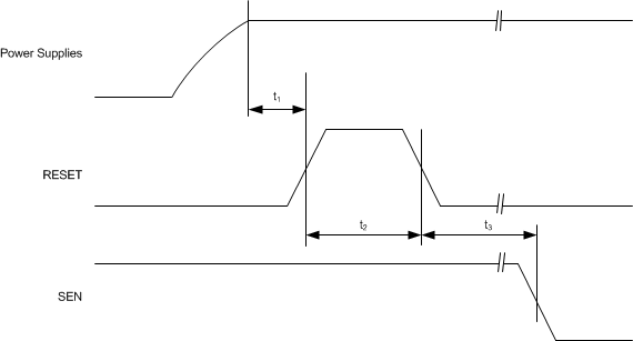 Figure 130. Hardware Reset Timing Diagram
Table 64. Timing Requirements for Figure 130
| MIN | TYP | MAX | UNIT | |||
|---|---|---|---|---|---|---|
| t1 | Power-on delay from power-up to an active high RESET pulse | 1 | ms | |||
| t2 | Reset pulse duration: active high RESET pulse duration | 10 | ns | |||
| t3 | Register write delay from RESET disable to SEN active | 100 | µs | |||
8.1.3 Frequency Planning
The ADS54J64 uses an architecture where the ADCs are 2x interleaved followed by a digital decimation by 2. The 2x interleaved and decimation architecture comes with a unique advantage of improved linearity resulting from frequency planning. Frequency planning refers to choosing the clock frequency and signal band appropriately such that the harmonic distortion components, resulting from the analog front-end (LNA, PGA), can be made to fall outside the decimation filter pass band. In absence of the 2x interleave and decimation architecture, these components alias back in band and limit the performance of the signal chain. For example, for fCLK = 983.04 MHz and fIN = 184.32 MHz:
Second-order harmonic distortion (HD2) = 2 × 184.32 = 368.64 MHz
Pass band of the 2x decimation filter = 0 MHz to 245.76 MHz (0 to fCLK / 4)
The second-order harmonic performance improves by the stop-band attenuation of the filter (approximately 40 dBc) because the second-order harmonic frequency is outside the pass band of the decimation filter.
Figure 131 shows the harmonic components (HD2–HD5) that fall in the decimation pass band for the input clock rate (fCLK) of the 983.04-MHz and 100-MHz signal band around the center frequency of 184.32 MHz.
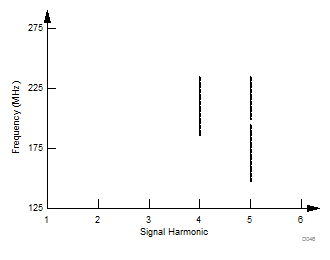
NOTE:
fCLK = 983.04 MHz, signal band = 134.32 MHz to 234.32 MHz.As shown in Figure 131, both HD2 and HD3 are completely out of band. HD4 and HD5 fall in the decimation pass band for some frequencies of the input signal band.
Through proper frequency planning, the specifications of the ADC antialias filter can be relaxed.
8.1.4 SNR and Clock Jitter
The signal-to-noise ratio of the ADC is limited by three different factors (as shown in Equation 3): the quantization noise is typically not noticeable in pipeline converters and is 84 dB for a 14-bit ADC. The thermal noise limits the SNR at low input frequencies and the clock jitter sets the SNR for higher input frequencies.

Equation 4 calculates the SNR limitation resulting from sample clock jitter:

The total clock jitter (TJitter) has two components: the internal aperture jitter (100 fS for the ADS54J64) that is set by the noise of the clock input buffer and the external clock jitter. Equation 5 calculates TJitter:

External clock jitter can be minimized by using high-quality clock sources and jitter cleaners as well as band-pass filters at the clock input; a faster clock slew rate also improves the ADC aperture jitter.
The ADS54J64 has a thermal noise of approximately 70 dBFS and an internal aperture jitter of 100 fS.
8.1.5 ADC Test Pattern
The ADS54J64 provides several different options to output test patterns instead of the actual output data of the ADC in order to simplify debugging of the JESD204B digital interface link. Figure 132 shows the output data path.
 Figure 132. ADC Test Pattern
8.1.5.1 ADC Section
The ADC test pattern replaces the actual output data of the ADC. These test patterns can be programmed using register 91h of the DIGTOP page. Table 65 lists the supported test patterns.
Table 65. ADC Test Pattern Settings
| BIT | NAME | DEFAULT | DESCRIPTION |
|---|---|---|---|
| 7-4 | TESTPATTERNSELECT | 0000 | These bits select the test pattern on the output when the test pattern is enabled for a suitable channel. 0 : Default 1 : All zeros 2 : All ones 3 : Toggle pattern 4 : Ramp pattern 6 : Custom pattern 1 7 : Toggles between custom pattern 1 and custom pattern 2 8 : Deskew pattern (AAAAh) |
8.1.5.2 Transport Layer Pattern
The transport layer maps the ADC output data into 8-bit octets and constructs the JESD204B frames using the LMFS parameters. Tail bits or 0s are added when needed. Alternatively, as shown in Table 66, the JESD204B long transport layer test pattern can be substituted by programming register 20h.
Table 66. Transport Layer Test Mode
| BIT | NAME | DEFAULT | DESCRIPTION |
|---|---|---|---|
| 4 | TRANS_TEST_EN | 0 | This bit generates the long transport layer test pattern mode according to clause 5.1.6.3 of the JESD204B specification. 0 = Test mode disabled 1 = Test mode enabled |
8.1.5.3 Link Layer Pattern
The link layer contains the scrambler and the 8b, 10b encoding of any data passed on from the transport layer. Additionally, the link layer also handles the initial lane alignment sequence that can be manually restarted. The link layer test patterns are intended for testing the quality of the link (jitter testing and so forth). The test patterns do not pass through the 8b, 10b encoder. These test patterns can be used by programming register 22h of the SERDES_XX page. Table 67 shows the supported programming options.
Table 67. Link Layer Test Mode
| BIT | NAME | DEFAULT | DESCRIPTION |
|---|---|---|---|
| 7-5 | LINK_LAYER_TESTMODE_SEL | 000 | These bits generate a pattern according to clause 5.3.3.8.2 of the JESD204B document. 0 : Normal ADC data 1 : D21.5 (high-frequency jitter pattern) 2 : K28.5 (mixed-frequency jitter pattern) 3 : Repeats initial lane alignment (generates a K28.5 character and continuously repeats lane alignment sequences) 4 : 12-octet RPAT jitter pattern 6 : PRBS pattern (PRBS7,15,23,31); use PRBS mode (register 36h) to select the PRBS pattern |
8.2 Typical Application
The ADS54J64 is designed for wideband receiver applications demanding excellent dynamic range over a large input frequency range. Figure 133 shows a typical schematic for an ac-coupled dual receiver [dual field-programmable gate array (FPGA) with a dual SYNC].
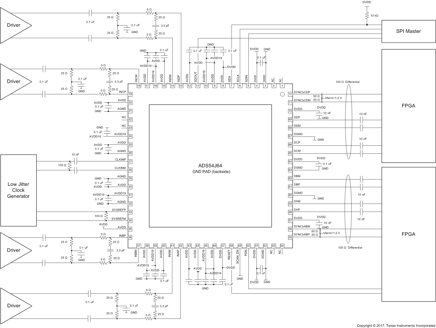
NOTE:
GND = AGND and DGND are connected in the PCB layout.8.2.1 Design Requirements
By using the simple drive circuit of Figure 133 (when the amplifier drives the ADC) or Figure 46 (when transformers drive the ADC), uniform performance can be obtained over a wide frequency range. The buffers present at the analog inputs of the device help isolate the external drive source from the switching currents of the sampling circuit.
8.2.2 Detailed Design Procedure
For optimum performance, the analog inputs must be driven differentially. This architecture improves the common-mode noise immunity and even-order harmonic rejection. A small resistor (5 Ω to 10 Ω) in series with each input pin, as shown in Figure 133, is recommended to damp out ringing caused by package parasitics.
8.2.3 Application Curves
Figure 134 and Figure 135 show the typical performance at 190 MHz and 230 MHz, respectively.
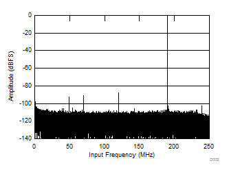
| fIN = 190 MHz, AIN = –1 dBFS, SNR = 69.4 dBFS, SFDR = 88 dBc, SFDR = 96 dBc (non 23) |
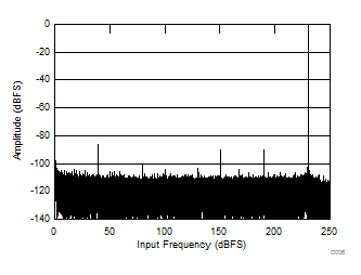
| fIN = 230 MHz, AIN = –1 dBFS, SNR = 69.4 dBFS, SFDR = 85 dBc, SFDR = 96 dBc (non 23) |