ZHCSEE2B December 2015 – January 2023 ADS54J66
PRODUCTION DATA
- 1 特性
- 2 应用
- 3 说明
- 4 Revision History
- 5 Pin Configuration and Functions
-
6 Specifications
- 6.1 Absolute Maximum Ratings
- 6.2 ESD Ratings
- 6.3 Recommended Operating Conditions
- 6.4 Thermal Information
- 6.5 Electrical Characteristics
- 6.6 AC Performance
- 6.7 Digital Characteristics
- 6.8 Timing Requirements
- 6.9 Typical Characteristics: General (DDC Mode-8)
- 6.10 Typical Characteristics: Mode 2
- 6.11 Typical Characteristics: Mode 0
-
7 Detailed Description
- 7.1 Overview
- 7.2 Functional Block Diagram
- 7.3 Feature Description
- 7.4
Device Functional Modes
- 7.4.1 Digital Features
- 7.4.2 Mode 0, Decimation-by-2 with IQ Outputs for up to 220 MHz of IQ Bandwidth
- 7.4.3 Mode 2, Decimation-by-2 for up to 110 MHz of Real Bandwidth
- 7.4.4 Modes 4 and 7, Decimation-by-2 with Real Outputs for up to 110 MHz of Bandwidth
- 7.4.5 Mode 5, Decimation-by-2 with IQ Outputs for up to 110 MHz of IQ Bandwidth
- 7.4.6 Mode 6, Decimation-by-4 with IQ Outputs for up to 110 MHz of IQ Bandwidth
- 7.4.7 Overrange Indication
- 7.4.8 Power-Down Mode
- 7.5 Programming
- 7.6
Register Maps
- 7.6.1 Detailed Register Information
- 7.6.2 Example Register Writes
- 7.6.3
Register Descriptions
- 7.6.3.1 General Registers
- 7.6.3.2
Master Page (80h)
- 7.6.3.2.1 Register 20h (address = 20h) [reset = 0h], Master Page (080h)
- 7.6.3.2.2 Register 21h (address = 21h) [reset = 0h], Master Page (080h)
- 7.6.3.2.3 Register 23h (address = 23h), Master Page (080h)
- 7.6.3.2.4 Register 24h (address = 24h) [reset = 0h], Master Page (080h)
- 7.6.3.2.5 Register 26h (address = 26h), Master Page (080h)
- 7.6.3.2.6 Register 3Ah (address = 3Ah) [reset = 0h], Master Page (80h)
- 7.6.3.2.7 Register 39h (address = 39h) [reset = 0h], Master Page (80h)
- 7.6.3.2.8 Register 53h (address = 53h) [reset = 0h], Master Page (80h)
- 7.6.3.2.9 Register 54h (address = 54h) [reset = 0h], Master Page (80h)
- 7.6.3.2.10 Register 55h (address = 55h) [reset = 0h], Master Page (80h)
- 7.6.3.2.11 Register 56h (address = 56h) [reset = 0h], Master Page (80h)
- 7.6.3.2.12 Register 59h (address = 59h) [reset = 0h], Master Page (80h)
- 7.6.3.3
ADC Page (0Fh)
- 7.6.3.3.1 Register 5Fh (address = 5Fh) [reset = 0h], ADC Page (0Fh)
- 7.6.3.3.2 Register 60h (address = 60h) [reset = 0h], ADC Page (0Fh)
- 7.6.3.3.3 Register 61h (address = 61h) [reset = 0h], ADC Page (0Fh)
- 7.6.3.3.4 Register 6Ch (address = 6Ch) [reset = 0h], ADC Page (0Fh)
- 7.6.3.3.5 Register 6Dh (address = 6Dh) [reset = 0h], ADC Page (0Fh)
- 7.6.3.3.6 Register 74h (address = 74h) [reset = 0h], ADC Page (0Fh)
- 7.6.3.3.7 Register 75h (address = 75h) [reset = 0h], ADC Page (0Fh)
- 7.6.3.3.8 Register 76h (address = 76h) [reset = 0h], ADC Page (0Fh)
- 7.6.3.3.9 Register 77h (address = 77h) [reset = 0h], ADC Page (0Fh)
- 7.6.3.3.10 Register 78h (address = 78h) [reset = 0h], ADC Page (0Fh)
- 7.6.3.4 Interleaving Engine Page (6100h)
- 7.6.3.5 Decimation Filter Page (6141h) Registers
- 7.6.3.6
Main Digital Page (6800h) Registers
- 7.6.3.6.1 Register 0h (address = 0h) [reset = 0h], Main Digital Page (6800h)
- 7.6.3.6.2 Register 42h (address = 42h) [reset = 0h], Main Digital Page (6800h)
- 7.6.3.6.3 Register 4Eh (address = 4Eh) [reset = 0h], Main Digital Page (6800h)
- 7.6.3.6.4 Register ABh (address = ABh) [reset = 0h], Main Digital Page (6800h)
- 7.6.3.6.5 Register ADh (address = ADh) [reset = 0h], Main Digital Page (6800h)
- 7.6.3.6.6 Register F7h (address = F7h) [reset = 0h], Main Digital Page (68h)
- 7.6.3.7
JESD Digital Page (6900h) Registers
- 7.6.3.7.1 Register 0h (address = 0h) [reset = 0h], JESD Digital Page (6900h)
- 7.6.3.7.2 Register 1h (address = 1h) [reset = 0h], JESD Digital Page (6900h)
- 7.6.3.7.3 Register 2h (address = 2h) [reset = 0h], JESD Digital Page (6900h)
- 7.6.3.7.4 Register 3h (address = 3h) [reset = 0h], JESD Digital Page (6900h)
- 7.6.3.7.5 Register 5h (address = 5h) [reset = 0h], JESD Digital Page (6900h)
- 7.6.3.7.6 Register 6h (address = 6h) [reset = 0h], JESD Digital Page (6900h)
- 7.6.3.7.7 Register 21h (address = 21h) [reset = 0h], JESD Digital Page (6900h)
- 7.6.3.7.8 Register 22h (address = 22h) [reset = 0h], JESD Digital Page (6900h)
- 7.6.3.8
JESD Analog Page (6A00h) Register
- 7.6.3.8.1 Register 12h, 13h (address 12h, 13h) [reset = 0h], JESD Analog Page (6Ah)
- 7.6.3.8.2 Register 16h (address = 16h) [reset = 0h], JESD Analog Page (6A00h)
- 7.6.3.8.3 Register 17h (address = 17h) [reset = 0h], JESD Analog Page (6A00h)
- 7.6.3.8.4 Register 1Bh (address = 1Bh) [reset = 0h], JESD Analog Page (6A00h)
- 8 Application Information Disclaimer
- 9 Device and Documentation Support
- 10Mechanical, Packaging, and Orderable Information
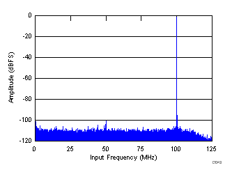
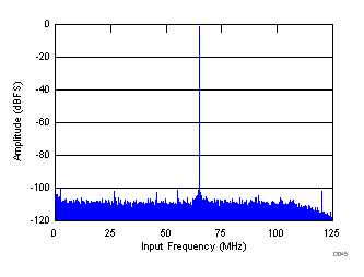
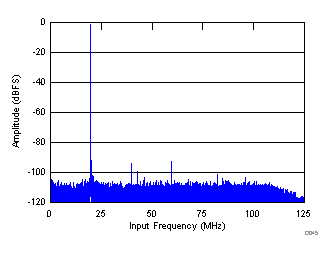
6.10 Typical Characteristics: Mode 2
low-pass or high-pass decimation-by-2 filter selected as per input frequency; typical values are at TA = 25°C, full temperature range is from TMIN = –40°C to TMAX = 85°C, ADC sampling frequency = 500 MSPS, 14-bit resolution, no decimation filter, 50% clock duty cycle, AVDD3V = 3 V, AVDD = DVDD = 1.9 V, IOVDD = 1.15 V, –1-dBFS differential input for IF ≤ 250 MHz, and –3-dBFS differential input for IF > 250 MHz (unless otherwise noted)

| fIN = 100 MHz, AIN = –1 dBFS, SNR = 74.1 dBFS, SFDR = 98 dBc, SFDR = 100 dBc (non 23) |

| fIN = 185 MHz, AIN = – 1 dBFS, SNR = 73.2 dBFS, SFDR = 98 dBc, SFDR = 98 dBc (non 23) |

| fIN = 150 MHz, AIN = –1 dBFS, SNR = 73.8 dBFS, SFDR = 99 dBc, SFDR = 99 dBc (non 23) |

| fIN = 230 MHz, AIN = –1 dBFS, SNR = 72.4 dBFS, SFDR = 91 dBc, SFDR = 98 dBc (non 23) |