ZHCSAM3B December 2012 – April 2022 ADS54T01
PRODUCTION DATA
- 1 特性
- 2 应用
- 3 说明
- 4 Revision History
- 5 Device Comparison
- 6 Pin Configuration and Functions
- 7 Specifications
-
8 Detailed Description
- 8.1 Overview
- 8.2 Functional Block Diagram
- 8.3
Feature Description
- 8.3.1 Test Pattern Output
- 8.3.2 Clock Inputs
- 8.3.3 SNR and Clock Jitter
- 8.3.4 Analog Inputs
- 8.3.5 Over-Range Indication
- 8.3.6 Interleaving Correction
- 8.3.7 High-Resolution Output Data
- 8.3.8 Low-Resolution Output Data
- 8.3.9 Full Speed – 7 Bit
- 8.3.10 Decimated Low-Resolution Output Data
- 8.3.11 Multi Device Synchronization
- 8.4 Device Functional Modes
- 8.5 Programming
- 8.6 Register Maps
- 9 Power Supply Recommendations
- 10Device and Documentation Support
- 11Mechanical, Packaging, and Orderable Information
7.9 Electrical Characteristics
The DC specifications refer to the condition where the digital outputs are not switching, but are permanently at a valid logic level 0 or 1. AVDD33 = 3.3 V, AVDDC/AVDD18/DVDD/DVDDLVDS/IOVDD = 1.8 V
| PARAMETER | TEST CONDITIONS | MIN | TYP | MAX | UNITS | |
|---|---|---|---|---|---|---|
| DIGITAL INPUTS – SRESET, SCLK, SDENB, SDIO, ENABLE | ||||||
| High-level input voltage | All digital inputs support 1.8-V and 3.3-V logic levels. | 0.7 x IOVDD | V | |||
| Low-level input voltage | 0.3 x IOVDD | V | ||||
| High-level input current | –50 | 200 | µA | |||
| Low-level input current | –50 | 50 | µA | |||
| Input capacitance | 5 | pF | ||||
| DIGITAL OUTPUTS – SDO | ||||||
| High-level output voltage | Iload = -100 µA | IOVDD – 0.2 | V | |||
| Iload = -2 mA | 0.8 x IOVDD | |||||
| Low-level output voltage | Iload = 100 µA | 0.2 | V | |||
| Iload = 2 mA | 0.22 x IOVDD | |||||
| DIGITAL INPUTS – SYNCP/N, TRIGGERP/N | ||||||
| VID | Differential input voltage | 250 | 350 | 450 | mV | |
| VCM | Input common-mode voltage | 1.125 | 1.2 | 1.375 | V | |
| tSU | 500 | ps | ||||
| DIGITAL OUTPUTS – DA[11:0]P/N, DACLKP/N, OVRAP/N, SYNCOUTP/N, TRDYP/N, HRESP/N | ||||||
| VOD | Output differential voltage | Iout = 3.5 mA | 250 | 350 | 450 | mV |
| VOCM | Output common-mode voltage | Iout = 3.5 mA | 1.125 | 1.25 | 1.375 | V |
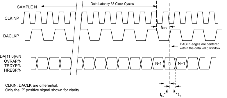
| tsu | Fs = 750 Msps | Data valid to zero-crossing of DACLK | 320 | 400 | ps | |
| th | Fs = 750 Msps | Zero-crossing of DACLK to data becoming invalid | 250 | 320 | ps | |
| tPD | Fs = 750Msps | CLKIN falling edge to DACLK rising edge | 3.36 | 3.69 | 3.92 | ns |
| tRISE | 10% - 90% | 100 | 150 | 200 | ps | |
| tFALL | 90% - 10% | 100 | 150 | 200 | ps | |
 Figure 7-1 Timing Diagram for 12-Bit DDR Output