ZHCSAM3B December 2012 – April 2022 ADS54T01
PRODUCTION DATA
- 1 特性
- 2 应用
- 3 说明
- 4 Revision History
- 5 Device Comparison
- 6 Pin Configuration and Functions
- 7 Specifications
-
8 Detailed Description
- 8.1 Overview
- 8.2 Functional Block Diagram
- 8.3
Feature Description
- 8.3.1 Test Pattern Output
- 8.3.2 Clock Inputs
- 8.3.3 SNR and Clock Jitter
- 8.3.4 Analog Inputs
- 8.3.5 Over-Range Indication
- 8.3.6 Interleaving Correction
- 8.3.7 High-Resolution Output Data
- 8.3.8 Low-Resolution Output Data
- 8.3.9 Full Speed – 7 Bit
- 8.3.10 Decimated Low-Resolution Output Data
- 8.3.11 Multi Device Synchronization
- 8.4 Device Functional Modes
- 8.5 Programming
- 8.6 Register Maps
- 9 Power Supply Recommendations
- 10Device and Documentation Support
- 11Mechanical, Packaging, and Orderable Information
8.3.4 Analog Inputs
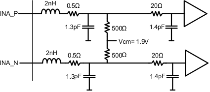
The ADS54T01 analog signal input is designed to be driven differentially. The analog input pins have internal analog buffers that drive the sampling circuit. As a result of the analog buffer, the input pins present a high impedance input across a very wide frequency range to the external driving source which enables great flexibility in the external analog filter design as well as excellent 50 Ω matching for RF applications. The buffer also helps isolate the external driving circuit from the internal switching currents of the sampling circuit which results in a more constant SFDR performance across input frequencies.
The common-mode voltage of the signal inputs is internally biased to 1.9 V using 500-Ω resistors which allows for AC coupling of the input drive network. Each input pin (INP, INM) must swing symmetrically between (VCM + 0.25 V) and (VCM – 0.25 V), resulting in a 1.0 Vpp (default) differential input swing. The input sampling circuit has a 3-dB bandwidth that extends up to 1.2 GHz.
 Figure 8-5 Analog Input Internal Circuitry