ZHCSAM3B December 2012 – April 2022 ADS54T01
PRODUCTION DATA
- 1 特性
- 2 应用
- 3 说明
- 4 Revision History
- 5 Device Comparison
- 6 Pin Configuration and Functions
- 7 Specifications
-
8 Detailed Description
- 8.1 Overview
- 8.2 Functional Block Diagram
- 8.3
Feature Description
- 8.3.1 Test Pattern Output
- 8.3.2 Clock Inputs
- 8.3.3 SNR and Clock Jitter
- 8.3.4 Analog Inputs
- 8.3.5 Over-Range Indication
- 8.3.6 Interleaving Correction
- 8.3.7 High-Resolution Output Data
- 8.3.8 Low-Resolution Output Data
- 8.3.9 Full Speed – 7 Bit
- 8.3.10 Decimated Low-Resolution Output Data
- 8.3.11 Multi Device Synchronization
- 8.4 Device Functional Modes
- 8.5 Programming
- 8.6 Register Maps
- 9 Power Supply Recommendations
- 10Device and Documentation Support
- 11Mechanical, Packaging, and Orderable Information
8.3.10 Decimated Low-Resolution Output Data
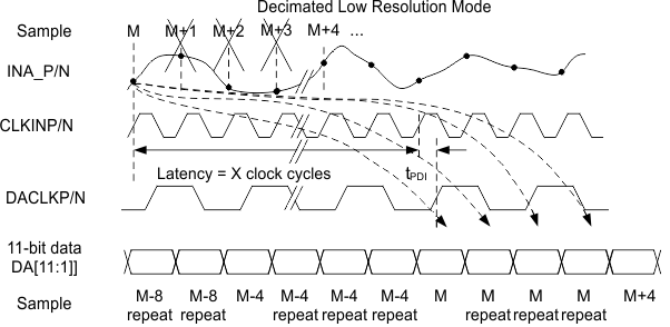
In decimated low-resolution mode, the output data is limited to 11 bits and every sample is repeated four times, so the effective data rate is 1/4 of ADC sampling rate. The latency of the ADC sample to output sample is exactly the same as for high-resolution data—there is no uncertainty in which conversion sample results in the valid output data. This is because the output continues to run at the ADC sample rate in decimated low-resolution mode where only the resolution is changed and three out of four samples are deleted.
 Figure 8-11 Decimated Low-Resolution Output Data Timing Diagram