ZHCSAM3B December 2012 – April 2022 ADS54T01
PRODUCTION DATA
- 1 特性
- 2 应用
- 3 说明
- 4 Revision History
- 5 Device Comparison
- 6 Pin Configuration and Functions
- 7 Specifications
-
8 Detailed Description
- 8.1 Overview
- 8.2 Functional Block Diagram
- 8.3
Feature Description
- 8.3.1 Test Pattern Output
- 8.3.2 Clock Inputs
- 8.3.3 SNR and Clock Jitter
- 8.3.4 Analog Inputs
- 8.3.5 Over-Range Indication
- 8.3.6 Interleaving Correction
- 8.3.7 High-Resolution Output Data
- 8.3.8 Low-Resolution Output Data
- 8.3.9 Full Speed – 7 Bit
- 8.3.10 Decimated Low-Resolution Output Data
- 8.3.11 Multi Device Synchronization
- 8.4 Device Functional Modes
- 8.5 Programming
- 8.6 Register Maps
- 9 Power Supply Recommendations
- 10Device and Documentation Support
- 11Mechanical, Packaging, and Orderable Information
8.3.6 Interleaving Correction
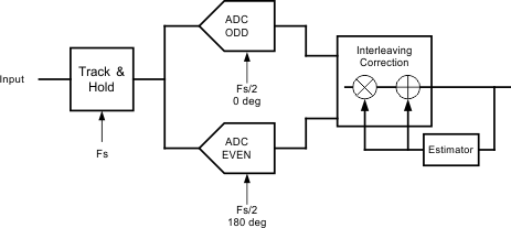
The data converter channel consists of two interleaved ADCs each operating at half of the ADC sampling rate but 180° out of phase from each other. The front end track and hold circuitry is operating at the full ADC sampling rate which minimizes the timing mismatch between the two interleaved ADCs. In addition, the ADS54T01 is equipped with internal interleaving correction logic that can be enabled through a SPI register write.
 Figure 8-7 Interleaving Correction Block Diagram
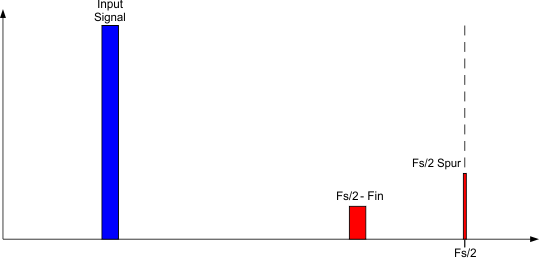
The interleaving operation creates 2 distinct and interleaving products:
- Fs/2 – Fin: this spur is created by gain timing mismatch between the ADCs. Since internally the front end track and hold is operated at the full sampling rate, this component is greatly improved and mostly dependent on gain mismatch.
- Fs/2 Spur: due to offset mismatch between ADCs
 Figure 8-8 Interleaving Correction Spurs
The auto correction loop can be enabled through a SPI register write in address 0x01. By default, the auto correction function is disabled for lowest possible power consumption. The default settings for the auto correction function should work for most applications. However please contact Texas Instruments if further fine tuning of the algorithm is required.
The auto correction function yields best performance for input frequencies below 250 MHz.