ZHCSAM3B December 2012 – April 2022 ADS54T01
PRODUCTION DATA
- 1 特性
- 2 应用
- 3 说明
- 4 Revision History
- 5 Device Comparison
- 6 Pin Configuration and Functions
- 7 Specifications
-
8 Detailed Description
- 8.1 Overview
- 8.2 Functional Block Diagram
- 8.3
Feature Description
- 8.3.1 Test Pattern Output
- 8.3.2 Clock Inputs
- 8.3.3 SNR and Clock Jitter
- 8.3.4 Analog Inputs
- 8.3.5 Over-Range Indication
- 8.3.6 Interleaving Correction
- 8.3.7 High-Resolution Output Data
- 8.3.8 Low-Resolution Output Data
- 8.3.9 Full Speed – 7 Bit
- 8.3.10 Decimated Low-Resolution Output Data
- 8.3.11 Multi Device Synchronization
- 8.4 Device Functional Modes
- 8.5 Programming
- 8.6 Register Maps
- 9 Power Supply Recommendations
- 10Device and Documentation Support
- 11Mechanical, Packaging, and Orderable Information
8.5.1 Device Initialization
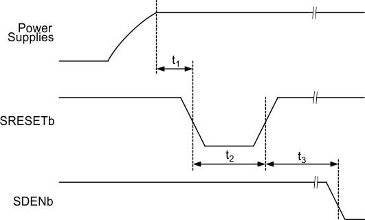
After power up, TI recommends to initialize the device through a hardware reset by applying a logic low pulse on the SRESETb pin (of width greater than 20 ns), as shown in Figure 8-19. This resets all internal digital blocks (including SPI registers) to their default condition.
 Figure 8-19 Device Initialization Timing Diagram
Table 8-5 Reset Timing
| PARAMETER | CONDITIONS | MIN | TYP | MAX | UNIT | |
|---|---|---|---|---|---|---|
| t1 | Power-on delay | Delay from power up to active low RESET pulse | 3 | ms | ||
| t2 | Reset pulse width | Active low RESET pulse width | 20 | ns | ||
| t3 | Register write delay | Delay from RESET disable to SDENb active | 100 | ns | ||
Recommended Device Initialization Sequence:
- Power up
- Reset ADS54T01 using hardware reset.
- Apply clock and input signal.
- Set register 0x01 bit D15 to "1" (ChA Corr EN) to enable gain/offset correction circuit and other desired registers.
- Set register 0x03 bit D14 to "1" (Start Auto Corr ChA). This clears and resets the accumulator values in the DC and gain correction loop.
- Set register 0x03 bit D14 to "0" (Start Auto Corr ChA). This starts the DC and gain auto-correction loop.