ZHCSAM3B December 2012 – April 2022 ADS54T01
PRODUCTION DATA
- 1 特性
- 2 应用
- 3 说明
- 4 Revision History
- 5 Device Comparison
- 6 Pin Configuration and Functions
- 7 Specifications
-
8 Detailed Description
- 8.1 Overview
- 8.2 Functional Block Diagram
- 8.3
Feature Description
- 8.3.1 Test Pattern Output
- 8.3.2 Clock Inputs
- 8.3.3 SNR and Clock Jitter
- 8.3.4 Analog Inputs
- 8.3.5 Over-Range Indication
- 8.3.6 Interleaving Correction
- 8.3.7 High-Resolution Output Data
- 8.3.8 Low-Resolution Output Data
- 8.3.9 Full Speed – 7 Bit
- 8.3.10 Decimated Low-Resolution Output Data
- 8.3.11 Multi Device Synchronization
- 8.4 Device Functional Modes
- 8.5 Programming
- 8.6 Register Maps
- 9 Power Supply Recommendations
- 10Device and Documentation Support
- 11Mechanical, Packaging, and Orderable Information
8.3.11 Multi Device Synchronization
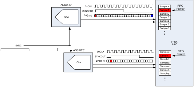
The ADS54T01 simplifies the synchronization of data from multiple ADCs in one common receiver. Upon receiving the initial SYNC input signal, the ADS54T01 resets all the internal clocks and digital logic while also starting a SYNCOUT signal which operates on a 5-bit counter (32 clock cycles). Therefore, by providing a common SYNC signal to multiple ADCs, their output data can be synchronized as the SYNCOUT signal marks a specific sample with the same latency in all ADCs. The SYNCOUT signal then can be used in the receiving device to synchronize the FIFO pointers across the different input data streams. Thus the output data of multiple ADCs can be aligned properly even if there are different trace lengths between the different ADCs.
 Figure 8-12 Multi Device SYNC
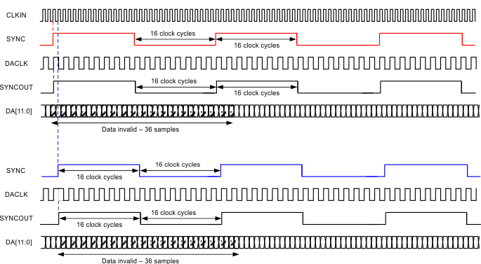
The SYNC input signal should be a one-time pulse to trigger the periodic 5-bit counter for SYNCOUT or a periodic signal repeating every 32 CLKIN clock cycles. The signal is registered on the rising edge of the ADC input clock (CLKIN). Upon registering the initial rising edge of the SYNC signal, the internal clocks and logic get reset which results in invalid output data for 36 samples (1 complete sync cycle and 4 additional samples). The SYNCOUT signal starts with the next output clock (DACLK) rising edge and operates on a 5-bit counter. If a SYNCIN rising edge gets registered at a new position, the counter gets reset and SYNCOUT starts from the new position.
The ADS54T01 output interface operates with a DDR clock, therefore the synchronization can happen on the rising edge or falling edge sample. Synchronization on the falling edge sample will result in a half cycle clock stretch of DACLK. For convenience, the SYNCOUT signal is available on the ChA output LVDS bus.
When using decimation, the SYNCOUT signal still operates on 32 clock cycles of CLKIN, but because the output data is decimated by 2, only the first 18 samples should be discarded.
 Figure 8-13 SYNC Timing Diagram