SLWS207B May 2008 – January 2016 ADS5560 , ADS5562
PRODUCTION DATA.
- 1 Features
- 2 Applications
- 3 Description
- 4 Revision History
- 5 Pin Configuration and Functions
-
6 Specifications
- 6.1 Absolute Maximum Ratings
- 6.2 ESD Ratings
- 6.3 Recommended Operating Conditions
- 6.4 Thermal Information
- 6.5 Electrical Characteristics
- 6.6 AC Electrical Characteristics for ADS5560 Fs = 40 MSPS
- 6.7 AC Electrical Characteristics for ADS5562, Fs = 80 MSPS
- 6.8 Electrical Characteristics for ADS5562
- 6.9 Electrical Characteristics for ADS5560
- 6.10 Digital Characteristics
- 6.11 Timing Characteristics for LVDS and CMOS Modes
- 6.12 Serial Interface Timing Characteristics
- 6.13 Reset Timing
- 6.14 Timing Characteristics at Lower Sampling Frequencies
- 6.15 Typical Characteristics
- 7 Detailed Description
- 8 Application and Implementation
- 9 Power Supply Recommendations
- 10Layout
- 11Device and Documentation Support
- 12Mechanical, Packaging, and Orderable Information
10 Layout
10.1 Layout Guidelines
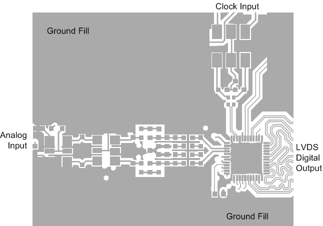
Figure 62 is a section of the layout of the ADS5562 that illustrates good layout practices for the clocking, analog input, and digital outputs. In this example, the analog input enters from the left while the clocking enters from the top, keeping the clock signal away from the analog signals so as to not allow coupling between the analog signal and the clock signal. On the layout of the differential traces, note the symmetry of the trace routing between the two sides of the differential signals.
The digital outputs are routed off to the right, so as to keep the digital signals away from the analog inputs and away from the clock. Note the circuitous routing added to some of the LVDS differential traces but not to others; this is the equalize the lengths of the routing across all of the LVDS traces so as to preserve the setup/hold timing at the end of the digital signal routings. If the timing closure in the receiving device (such as an FPGA or ASIC) has enough timing margin, then the circuitous routing to equalize trace lengths may not be necessary.
In addition, the solid gray areas are ground planes, providing more isolation between the clocking and the analog inputs as well as between the clocking and the digital outputs.
10.1.1 Supply Decoupling
As ADS556x already includes internal decoupling, minimal external decoupling can be used without loss in performance. Decoupling capacitors can help to filter external power supply noise, so the optimum number of capacitors would depend on the actual application. The decoupling capacitors should be placed very close to the converter supply pins. TI recommends using separate supplies for the analog and digital supply pins to isolate digital switching noise from sensitive analog circuitry. In case only a single 3.3-V supply is available, it should be routed first to AVDD. The supply can then be tapped and isolated with a ferrite bead (or inductor) with decoupling capacitor, before being routed to DRVDD.
10.2 Layout Example
 Figure 62. Typical Layout of ADS5562