ZHCSFX9 January   2017 ADS7029-Q1

PRODUCTION DATA.  

  1. 特性
  2. 应用
  3. 说明
  4. 修订历史记录
  5. Pin Configuration and Functions
  6. Specifications
    1. 6.1 Absolute Maximum Ratings
    2. 6.2 ESD Ratings
    3. 6.3 Recommended Operating Conditions
    4. 6.4 Thermal Information
    5. 6.5 Electrical Characteristics
    6. 6.6 Timing Requirements
    7. 6.7 Switching Characteristics
    8. 6.8 Typical Characteristics
  7. Parameter Measurement Information
    1. 7.1 Digital Voltage Levels
  8. Detailed Description
    1. 8.1 Overview
    2. 8.2 Functional Block Diagram
    3. 8.3 Feature Description
      1. 8.3.1 Reference
      2. 8.3.2 Analog Input
      3. 8.3.3 ADC Transfer Function
      4. 8.3.4 Serial Interface
    4. 8.4 Device Functional Modes
      1. 8.4.1 Offset Calibration
        1. 8.4.1.1 Offset Calibration on Power-Up
        2. 8.4.1.2 Offset Calibration During Normal Operation
  9. Application and Implementation
    1. 9.1 Application Information
    2. 9.2 Typical Application
      1. 9.2.1 Design Requirements
      2. 9.2.2 Detailed Design Procedure
        1. 9.2.2.1 Low Distortion Charge Kickback Filter Design
        2. 9.2.2.2 Input Amplifier Selection
        3. 9.2.2.3 Reference Circuit
      3. 9.2.3 Application Curve
  10. 10Power Supply Recommendations
    1. 10.1 AVDD and DVDD Supply Recommendations
    2. 10.2 Estimating Digital Power Consumption
    3. 10.3 Optimizing Power Consumed by the Device
  11. 11Layout
    1. 11.1 Layout Guidelines
    2. 11.2 Layout Example
  12. 12器件和文档支持
    1. 12.1 文档支持
      1. 12.1.1 相关文档 
    2. 12.2 接收文档更新通知
    3. 12.3 社区资源
    4. 12.4 商标
    5. 12.5 静电放电警告
    6. 12.6 Glossary
  13. 13机械、封装和可订购信息

封装选项

机械数据 (封装 | 引脚)
散热焊盘机械数据 (封装 | 引脚)
订购信息

Layout

Layout Guidelines

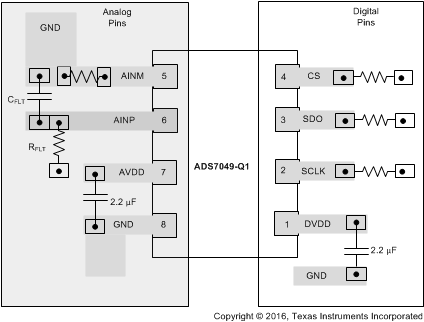
Figure 41 shows a board layout example for the ADS7029-Q1.

Some of the key considerations for an optimum layout with this device are:

  • Use a ground plane underneath the device and partition the printed circuit board (PCB) into analog and digital sections.
  • Avoid crossing digital lines with the analog signal path and keep the analog input signals and the reference input signals away from noise sources.
  • The power sources to the device must be clean and well-bypassed. Use 2.2-μF ceramic bypass capacitors in close proximity to the analog (AVDD) and digital (DVDD) power-supply pins.
  • Avoid placing vias between the AVDD and DVDD pins and the bypass capacitors.
  • Connect ground pins to the ground plane using short, low-impedance path.
  • Place the fly-wheel RC filters components close to the device.

Among ceramic surface-mount capacitors, COG (NPO) ceramic capacitors provide the best capacitance precision. The type of dielectric used in COG (NPO) ceramic capacitors provides the most stable electrical properties over voltage, frequency, and temperature changes.

Layout Example

ADS7029-Q1 layout_sbas763.gif Figure 41. Example Layout