ZHCSD02D November 2014 – December 2015 ADS7043
PRODUCTION DATA.
- 1 特性
- 2 应用
- 3 说明
- 4 修订历史记录
- 5 Pin Configuration and Functions
- 6 Specifications
- 7 Parameter Measurement Information
- 8 Detailed Description
- 9 Application and Implementation
- 10Power-Supply Recommendations
- 11Layout
- 12器件和文档支持
- 13机械、封装和可订购信息
封装选项
请参考 PDF 数据表获取器件具体的封装图。
机械数据 (封装 | 引脚)
- DCU|8
- RUG|8
散热焊盘机械数据 (封装 | 引脚)
订购信息
11 Layout
11.1 Layout Guidelines
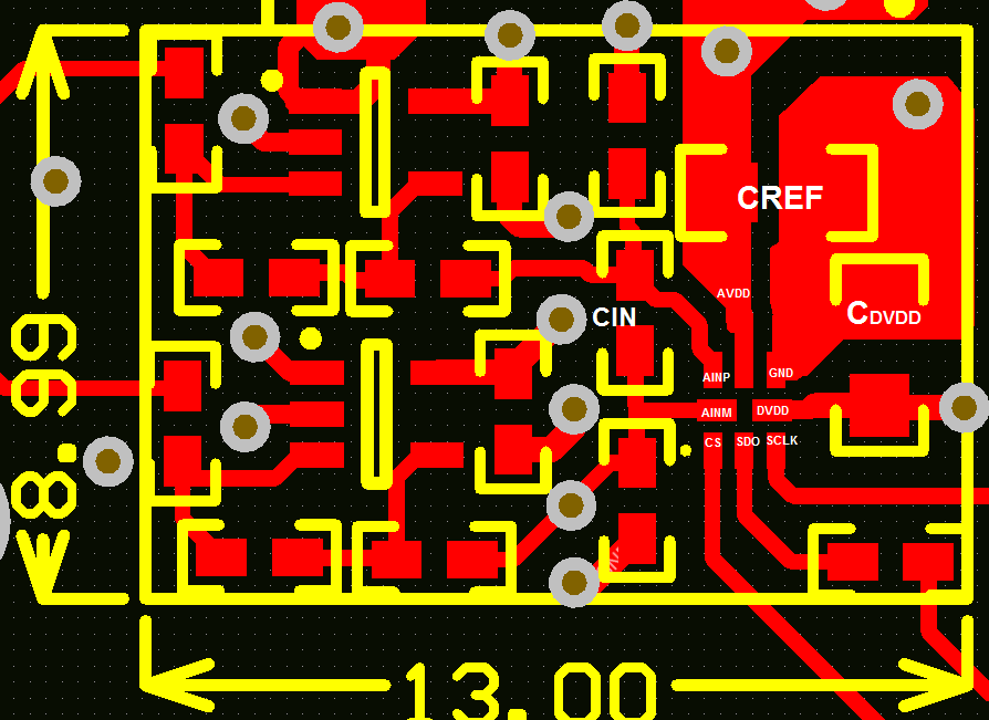
Figure 45 shows a board layout example for the ADS7043. Use a ground plane underneath the device and partition the PCB into analog and digital sections. Avoid crossing digital lines with the analog signal path and keep the analog input signals and the reference input signals away from noise sources. In Figure 45, the analog input and reference signals are routed on the top and left side of the device while the digital connections are routed on the bottom and right side of the device.
The power sources to the device must be clean and well-bypassed. Use 1-μF ceramic bypass capacitors in close proximity to the analog (AVDD) and digital (DVDD) power-supply pins. Avoid placing vias between the AVDD and DVDD pins and the bypass capacitors. Connect all ground pins to the ground plane using short, low-impedance paths. The AVDD supply voltage for the ADS7043 also functions as a reference for the device. Place the decoupling capacitor (CREF) for AVDD close to the device AVDD and GND pins. CREF must be connected to the device pins with thick copper tracks, as shown in Figure 45.
The fly-wheel RC filters are placed close to the device. Among ceramic surface-mount capacitors, COG (NPO) ceramic capacitors provide the best capacitance precision. The type of dielectric used in COG (NPO) ceramic capacitors provides the most stable electrical properties over voltage, frequency, and temperature changes.
11.2 Layout Example
 Figure 45. Example Layout