ZHCSH50 December   2016 ADS7046

PRODUCTION DATA.  

  1. 特性
  2. 应用
  3. 说明
  4. 修订历史记录
  5. Pin Configuration and Functions
  6. Specifications
    1. 6.1 Absolute Maximum Ratings
    2. 6.2 ESD Ratings
    3. 6.3 Recommended Operating Conditions
    4. 6.4 Thermal Information
    5. 6.5 Electrical Characteristics
    6. 6.6 Timing Requirements
    7. 6.7 Switching Characteristics
    8. 6.8 Typical Characteristics
  7. Parameter Measurement Information
    1. 7.1 Digital Voltage Levels
  8. Detailed Description
    1. 8.1 Overview
    2. 8.2 Functional Block Diagram
    3. 8.3 Feature Description
      1. 8.3.1 Product Family
      2. 8.3.2 Analog Input
      3. 8.3.3 Reference
      4. 8.3.4 ADC Transfer Function
    4. 8.4 Device Functional Modes
      1. 8.4.1 ACQ State
      2. 8.4.2 CNV State
      3. 8.4.3 OFFCAL State
        1. 8.4.3.1 Offset Calibration on Power-Up
        2. 8.4.3.2 Offset Calibration During Normal Operation
  9. Application and Implementation
    1. 9.1 Application Information
    2. 9.2 Typical Applications
      1. 9.2.1 Single-Supply Data Acquisition With the ADS7046
        1. 9.2.1.1 Design Requirements
        2. 9.2.1.2 Detailed Design Procedure
          1. 9.2.1.2.1 Low Distortion Charge Kickback Filter Design
          2. 9.2.1.2.2 Input Amplifier Selection
          3. 9.2.1.2.3 Reference Circuit
        3. 9.2.1.3 Application Curves
      2. 9.2.2 High Bandwidth (1 MHz) Data Acquisition With the ADS7046
        1. 9.2.2.1 Design Requirements
        2. 9.2.2.2 Detailed Design Procedure
        3. 9.2.2.3 Application Curves
      3. 9.2.3 12-Bit, 10-kSPS DAQ Circuit Optimized for DC Sensor Measurements
        1. 9.2.3.1 Design Requirements
        2. 9.2.3.2 Detailed Design Procedure
        3. 9.2.3.3 Application Curve
  10. 10Power Supply Recommendations
    1. 10.1 AVDD and DVDD Supply Recommendations
    2. 10.2 Optimizing Power Consumed by the Device
      1. 10.2.1 Estimating Digital Power Consumption
  11. 11Layout
    1. 11.1 Layout Guidelines
    2. 11.2 Layout Example
  12. 12器件和文档支持
    1. 12.1 器件支持
      1. 12.1.1 开发支持
    2. 12.2 文档支持
      1. 12.2.1 相关文档
    3. 12.3 接收文档更新通知
    4. 12.4 社区资源
    5. 12.5 商标
    6. 12.6 静电放电警告
    7. 12.7 Glossary
  13. 13机械、封装和可订购信息

封装选项

机械数据 (封装 | 引脚)
散热焊盘机械数据 (封装 | 引脚)
订购信息

Layout

Layout Guidelines

Figure 50 shows a typical connection diagram for the ADS7046.
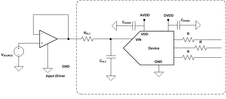
ADS7046 layout_sch_se_sbas769.gif Figure 50. Typical Connection Diagram

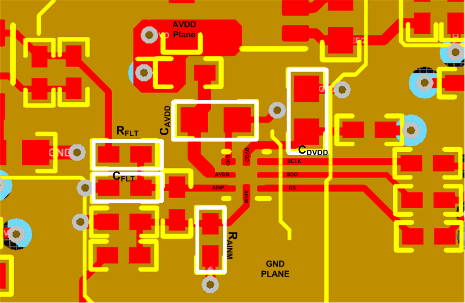
Figure 51 depicts a board layout example for the device for the typical connection diagram in Figure 50. The key considerations for layout are:

  • Use a solid ground plane underneath the device and partition the PCB into analog and digital sections
  • Avoid crossing digital lines with the analog signal path and keep the analog input signals and the reference input signals away from noise sources.
  • The power sources to the device must be clean and well-bypassed. Use CAVDD decoupling capacitors in close proximity to the analog (AVDD) power-supply pin.
  • Use a CDVDD decoupling capacitor close to the digital (DVDD) power-supply pin.
  • Avoid placing vias between the AVDD and DVDD pins and the bypass capacitors.
  • Connect the ground pin to the ground plane using a short, low-impedance path.
  • Place the charge kickback filter components close to the device.

Among ceramic surface-mount capacitors, COG (NPO) ceramic capacitors are recommended because these components provide the most stable electrical properties over voltage, frequency, and temperature changes.

Layout Example

ADS7046 layout_layout_se_sbas769.gif Figure 51. Example Layout