ZHCSFM9 November 2016 ADS7049-Q1
PRODUCTION DATA.
6 Specifications
6.1 Absolute Maximum Ratings(1)
| MIN | MAX | UNIT | |
|---|---|---|---|
| AVDD to GND | –0.3 | 3.9 | V |
| DVDD to GND | –0.3 | 3.9 | V |
| AINP to GND | –0.3 | AVDD + 0.3 | V |
| AINM to GND | –0.3 | 0.3 | V |
| Digital input voltage to GND | –0.3 | DVDD + 0.3 | V |
| Storage temperature, Tstg | –60 | 150 | °C |
(1) Stresses beyond those listed under Absolute Maximum Ratings may cause permanent damage to the device. These are stress ratings only, which do not imply functional operation of the device at these or any other conditions beyond those indicated under Recommended Operating Conditions. Exposure to absolute-maximum-rated conditions for extended periods may affect device reliability.
6.2 ESD Ratings
| VALUE | UNIT | |||
|---|---|---|---|---|
| V(ESD) | Electrostatic discharge | Human-body model (HBM), per AEC Q100-002(1) | ±2000 | V |
| Charged-device model (CDM), per AEC Q100-011 | ±1000 | |||
(1) AEC Q100-002 indicates that HBM stressing shall be in accordance with the ANSI/ESDA/JEDEC JS-001 specification.
6.3 Recommended Operating Conditions
over operating free-air temperature range (unless otherwise noted)| MIN | NOM | MAX | UNIT | ||
|---|---|---|---|---|---|
| AVDD | Analog supply voltage range | 2.35 | 3.6 | V | |
| DVDD | Digital supply voltage range | 1.65 | 3.6 | V | |
| TA | Operating free-air temperature | –40 | 125 | °C | |
6.4 Thermal Information
| THERMAL METRIC(1) | ADS7049-Q1 | UNIT | |
|---|---|---|---|
| DCU (VSSOP) | |||
| 8 PINS | |||
| RθJA | Junction-to-ambient thermal resistance | 181.8 | °C/W |
| RθJC(top) | Junction-to-case (top) thermal resistance | 50.8 | °C/W |
| RθJB | Junction-to-board thermal resistance | 73.9 | °C/W |
| ψJT | Junction-to-top characterization parameter | 1.0 | °C/W |
| ψJB | Junction-to-board characterization parameter | 73.9 | °C/W |
| RθJC(bot) | Junction-to-case (bottom) thermal resistance | N/A | °C/W |
(1) For more information about traditional and new thermal metrics, see the Semiconductor and IC Package Thermal Metrics application report.
6.5 Electrical Characteristics
at TA = –40°C to 125°C, AVDD = 3 V, DVDD = 1.65 V to 3.6 V, fSAMPLE = 2 MSPS, and VAINM = 0 V (unless otherwise noted)| PARAMETER | TEST CONDITIONS | MIN | TYP | MAX | UNIT | ||
|---|---|---|---|---|---|---|---|
| ANALOG INPUT | |||||||
| Full-scale input voltage span(1) | 0 | AVDD | V | ||||
| Absolute input voltage range | AINP to GND | –0.1 | AVDD + 0.1 | V | |||
| AINM to GND | –0.1 | 0.1 | |||||
| CS | Sampling capacitance | 15 | pF | ||||
| SYSTEM PERFORMANCE | |||||||
| Resolution | 12 | Bits | |||||
| NMC | No missing codes | 12 | Bits | ||||
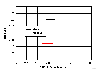
| INL | Integral nonlinearity | AVDD = 3 V | –1 | ±0.5 | 1 | LSB(2) | |
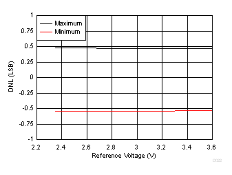
| DNL | Differential nonlinearity | AVDD = 3 V | –0.99 | ±0.5 | 1 | LSB | |
| EO | Offset error | Uncalibrated | ±12 | LSB | |||
| Calibrated(6) | AVDD = 3 V | –3 | ±0.5 | 3 | |||
| dVOS/dT | Offset error drift with temperature | ±5 | ppm/°C | ||||
| EG | Gain error | AVDD = 3 V | –0.1 | ±0.05 | 0.1 | %FS | |
| Gain error drift with temperature | No calibration | ±2 | ppm/°C | ||||
| SAMPLING DYNAMICS | |||||||
| tACQ | Acquisition time | 90 | ns | ||||
| Maximum throughput rate | 32-MHz SCLK, AVDD = 2.35 V to 3.6 V | 2 | MHz | ||||
| DYNAMIC CHARACTERISTICS | |||||||
| SNR | Signal-to-noise ratio(4) | fIN = 2 kHz, AVDD = 3 V | 68 | 70 | dB | ||
| THD | Total harmonic distortion(4)(3) | fIN = 2 kHz, AVDD = 3 V | –80 | dB | |||
| SINAD | Signal-to-noise and distortion(4) | fIN = 2 kHz, AVDD = 3 V | 67.5 | 69.5 | dB | ||
| SFDR | Spurious-free dynamic range(4) | fIN = 2 kHz, AVDD = 3 V | 80 | dB | |||
| BW(fp) | Full-power bandwidth | At –3 dB, AVDD = 3 V | 25 | MHz | |||
| DIGITAL INPUT/OUTPUT (CMOS Logic Family) | |||||||
| VIH | High-level input voltage(5) | 0.65 × DVDD | DVDD + 0.3 | V | |||
| VIL | Low-level input voltage(5) | –0.3 | 0.35 × DVDD | V | |||
| VOH | High-level output voltage(5) | At Isource = 500 µA | 0.8 × DVDD | DVDD | V | ||
| At Isource = 2 mA | DVDD – 0.45 | DVDD | |||||
| VOL | Low-level output voltage(5) | At Isink = 500 µA | 0 | 0.2 × DVDD | V | ||
| At Isink = 2 mA | 0 | 0.45 | |||||
| POWER-SUPPLY REQUIREMENTS | |||||||
| AVDD | Analog supply voltage | 2.35 | 3 | 3.6 | V | ||
| DVDD | Digital I/O supply voltage | 1.65 | 3 | 3.6 | V | ||
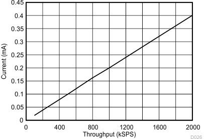
| IAVDD | Analog supply current | At 2 MSPS with AVDD = 3 V | 380 | 460 | µA | ||
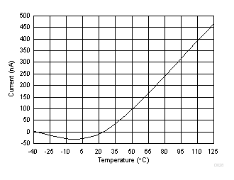
| IDVDD | Digital supply current | AVDD = 3 V, no load, no transitions | 10 | µA | |||
| PD | Power dissipation | At 2 MSPS with AVDD = 3 V | 1.14 | 1.38 | mW | ||
(1) Ideal input span; does not include gain or offset error.
(2) LSB means least significant bit.
(3) Calculated on the first nine harmonics of the input frequency.
(4) All specifications expressed in decibels (dB) refer to the full-scale input (FSR) and are tested with an input signal 0.5 dB below full-scale, unless otherwise specified.
(5) Digital voltage levels comply with the JESD8-7A standard for DVDD from 1.65 V to 1.95 V; see the Digital Voltage Levels section for more details.
(6) See the Offset Calibration section for more details.
6.6 Timing Requirements
all specifications are at TA = –40°C to 125°C, AVDD = 2.35 V to 3.6 V, DVDD = 1.65 V to 3.6 V, and CLOAD on SDO = 20 pF (unless otherwise specified)| MIN | TYP | MAX | UNIT | ||
|---|---|---|---|---|---|
| tACQ | Acquisition time | 90 | ns | ||
| fSCLK | SCLK frequency | 0.016 | 32 | MHz | |
| tSCLK | SCLK period | 31.25 | ns | ||
| tPH_CK | SCLK high time | 0.45 | 0.55 | tSCLK | |
| tPL_CK | SCLK low time | 0.45 | 0.55 | tSCLK | |
| tPH_CS | CS high time | 30 | ns | ||
| tSU_CSCK | Setup time: CS falling to SCLK falling | 12 | ns | ||
| tD_CKCS | Delay time: last SCLK falling to CS rising | 10 | ns | ||
6.7 Switching Characteristics
all specifications are at TA = –40°C to 125°C, AVDD = 2.35 V to 3.6 V, DVDD = 1.65 V to 3.6 V, and CLOAD on SDO = 20 pF (unless otherwise specified)| PARAMETER | TEST CONDITIONS | MIN | TYP | MAX | UNIT | |
|---|---|---|---|---|---|---|
| fTHROUGHPUT | Throughput | 2 | MSPS | |||
| tCYCLE | Cycle time | 0.5 | µs | |||
| tCONV | Conversion time | 12.5 × tSCLK + tSU_CSCK | ns | |||
| tDV_CSDO | Delay time: CS falling to data enable | 10 | ns | |||
| tD_CKDO | Delay time: SCLK falling to (next) data valid on DOUT | AVDD = 2.35 V to 3.6 V | 25 | ns | ||
| tDZ_CSDO | Delay time: CS rising to DOUT going to tri-state | 5 | ns | |||
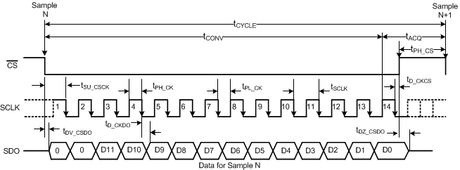 Figure 1. Timing Diagram
6.8 Typical Characteristics
at TA = 25°C, AVDD = 3 V, DVDD = 1.8 V, and fSAMPLE = 2 MSPS (unless otherwise noted)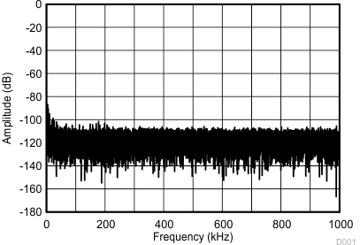
| SNR = 70.29 dB, THD = –84.04 dB, fIN = 2 kHz, number of samples = 65536 |
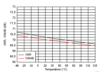
| fIN = 2 kHz |
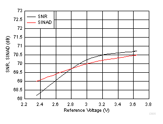
| fIN = 2 kHz |
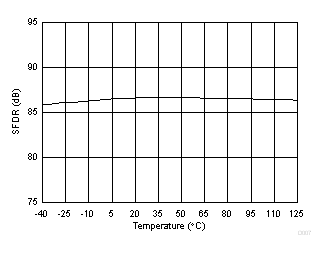
| fIN = 2 kHz |
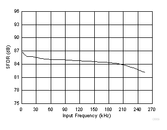
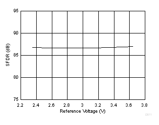
| fIN = 2 kHz |
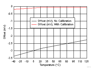
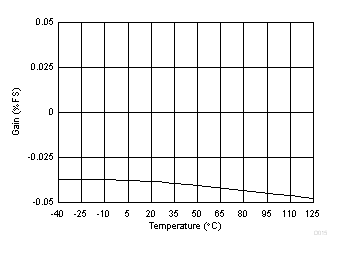
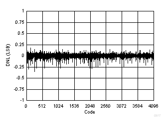
| AVDD = 3 V |
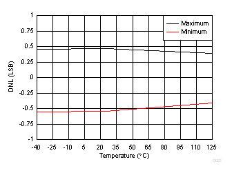
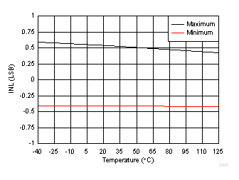
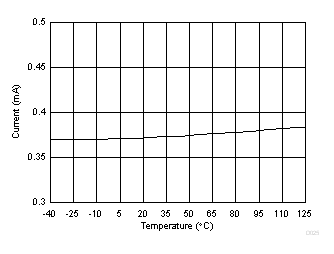
| fSample = 2 MSPS |
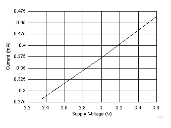
| fSample = 2 MSPS |
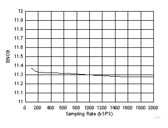
| fIN = 2 kHz |
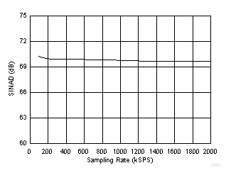
| fIN = 2 kHz |
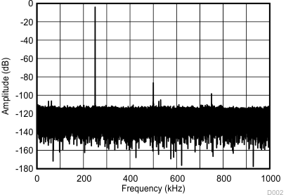
| SNR = 69.92 dB, THD = –80.05 dB, fIN = 250 kHz, number of samples = 65536 |
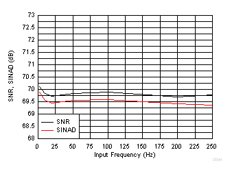
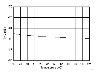
| fIN = 2 kHz |
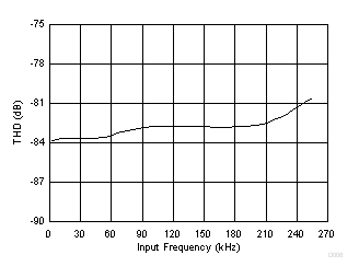
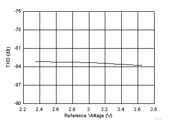
| fIN = 2 kHz |

| Mean code = 2046.92, sigma = 0.42 |
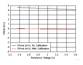
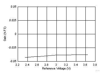
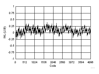
| AVDD = 3 V |
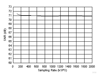
| fIN = 2 kHz |
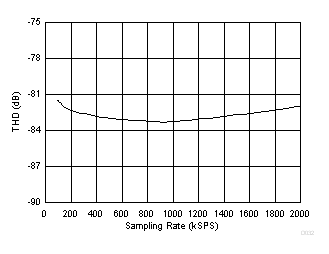
| fIN = 2 kHz |