ZHCSH54 December 2017 ADS7054
PRODUCTION DATA.
- 1 特性
- 2 应用
- 3 说明
- 4 修订历史记录
- 5 Pin Configuration and Functions
- 6 Specifications
- 7 Parameter Measurement Information
- 8 Detailed Description
- 9 Application and Implementation
- 10Power Supply Recommendations
- 11Layout
- 12器件和文档支持
- 13机械、封装和可订购信息
9 Application and Implementation
NOTE
Information in the following applications sections is not part of the TI component specification, and TI does not warrant its accuracy or completeness. TI’s customers are responsible for determining suitability of components for their purposes. Customers should validate and test their design implementation to confirm system functionality.
9.1 Application Information
The two primary supporting circuits required to maximize the performance of a high-precision, successive approximation register (SAR) analog-to-digital converter (ADC) are the input driver and the reference driver circuits. This section details some general principles for designing the input driver circuit, reference driver circuit, and provides typical application circuits designed for the device.
9.2 Typical Applications
9.2.1 2-Channel, Simultaneous Sampling Data Acquisition Using the ADS7054
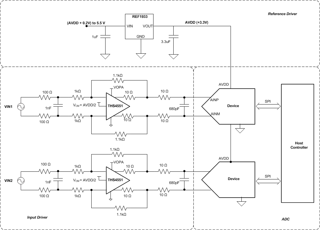 Figure 40. 2-Channel, Simultaneous-Sampling Data Acquisition (DAQ) Circuit Using the ADS7054
9.2.1.1 Design Requirements
The goal of the circuit shown in Figure 40 is to design a two-channel, simultaneous-sampling data acquisition (DAQ) circuit based on the ADS7054 with an SNR greater than 79 dB and a THD less than –85 dB for input frequencies from 2 kHz to 50 kHz at a throughput of 1 MSPS. This simultaneous-sampling scheme is typically used in motor sine and cosine (sin-cos) encoders, resolvers, fish finders, sonar, and I-Q demodulation.
9.2.1.2 Detailed Design Procedure
The input driver circuit for a high-precision ADC mainly consists of two parts: a driving amplifier and charge kickback filter. Careful design of the front-end circuit is critical to meet the linearity and noise performance of a high-precision ADC.
9.2.1.2.1 Low Distortion Charge Kickback Filter Design
Figure 41 shows the input circuit of a typical SAR ADC. During the acquisition phase, the SW switch closes and connects the sampling capacitor (CSH) to the input driver circuit. This action introduces a transient on the input pins of the SAR ADC. An ideal amplifier with 0 Ω of output impedance and infinite current drive can settle this transient in zero time. For a real amplifier with non-zero output impedance and finite drive strength, this switched capacitor load can create stability issues.
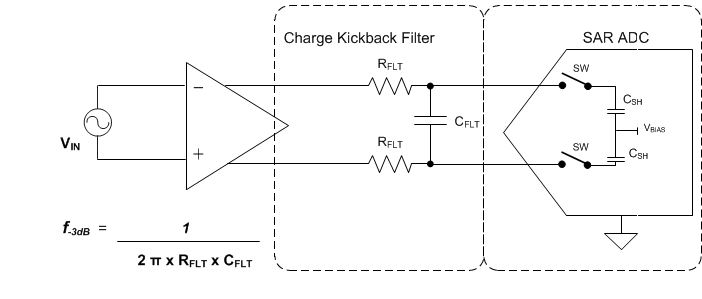 Figure 41. Input Sample-and-Hold Circuit for a Typical SAR ADC
For ac signals, the filter bandwidth must be kept low to band-limit the noise fed into the ADC input, thereby increasing the signal-to-noise ratio (SNR) of the system. Besides filtering the noise from the front-end drive circuitry, the RC filter also helps attenuate the sampling charge injection from the switched-capacitor input stage of the ADC. A filter capacitor, CFLT, is connected across the ADC inputs. This capacitor helps reduce the sampling charge injection and provides a charge bucket to quickly charge the internal sample-and-hold capacitors during the acquisition process. As a rule of thumb, the value of this capacitor is at least 20 times the specified value of the ADC sampling capacitance. For this device, the input sampling capacitance is equal to 16 pF. Thus, the value of CFLT is greater than 320 pF. Select a COG- or NPO-type capacitor because these capacitor types have a high-Q, low-temperature coefficient, and stable electrical characteristics under varying voltages, frequency, and time.
Driving capacitive loads can degrade the phase margin of the input amplifiers, thus making the amplifier marginally unstable. To avoid amplifier stability issues, series isolation resistors (RFLT) are used at the output of the amplifiers. A higher value of RFLT is helpful from the amplifier stability perspective, but adds distortion as a result of interactions with the nonlinear input impedance of the ADC. Distortion increases with source impedance, input signal frequency, and input signal amplitude. Therefore, the selection of RFLT requires balancing the stability and distortion of the design.
9.2.1.2.2 Input Amplifier Selection
The input amplifier bandwidth is typically much higher than the cutoff frequency of the charge kickback filter. Thus, TI strongly recommends performing a SPICE simulation to confirm that the amplifier has more than 40° phase margin with the selected filter. Simulation is critical because even with high-bandwidth amplifiers, some amplifiers can require more bandwidth than others to drive similar filters. To learn more about the SAR ADC input driver design, see the TI Precision Labs training video series.
The THS4551 is selected for its high bandwidth (135 MHz), low total harmonic distortion of –90 dBc at 100 kHz, and ultra-low noise of (3.2 nV/√Hz). The THS4551 is powered up from the power supply (VDD = 5 V and VSS = GND).
9.2.1.2.3 Reference Circuit
The ADS70xx uses the analog supply voltage (AVDD) as the reference voltage for the analog-to-digital conversion. During the conversion process, the internal capacitors are switched to the level of the AVDD pin as per the successive approximation algorithm. A voltage reference must be selected with low temperature drift, high output current drive, and low output impedance. For this application, the REF1933 was selected as the voltage reference and analog power supply for the ADC. The REF1933 has excellent temperature drift performance (25 ppm/°C), good initial accuracy (0.1%), high output drive capability (25 mA), and low quiescent current (360 µA). The REF1933 also provides a bias voltage output of half the reference voltage (VREF / 2) that can be used as the common-mode input for the amplifier.
TI recommends a 3.3-μF (CAVDD), low equivalent series resistance (ESR) ceramic capacitor between the AVDD and GND pins. This decoupling capacitor provides the instantaneous charge required by the internal circuit during the conversion process and maintains a stable dc voltage on the AVDD pin.
9.2.1.3 Application Curves
Figure 42 and Figure 43 provide the measurement results for the circuit described in Figure 40.
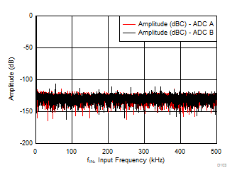
| Device 1 | SNR = 80.3 dB, THD = –93 dB, SINAD = 79.6 dB | ||
| Device 2 | SNR = 79.8 dB, THD = –92 dB, SINAD = 79.3 dB | ||
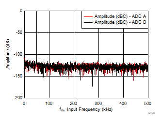
| Device 1 | SNR = 79.2 dB, THD = –94 dB, SINAD = 78.9 dB | ||
| Device 2 | SNR = 78.9 dB, THD = –92 dB, SINAD = 78.6 dB | ||
9.2.2 Improving Precision of Single-Ended Signal Source Measurements Using the ADS7054
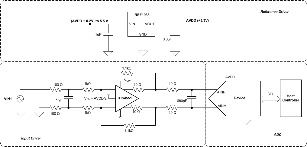 Figure 44. Interfacing Single-Ended Signals with the ADS7054 Using a Single-Ended to Differential
 Front-End
9.2.2.1 Design Requirements
Some applications have sensor or signal inputs that are single ended. In order to increase the dynamic range, linearity, and precision of the system, such single-ended signals are often required to be interfaced with a differential input ADC. The goal of the design shown in Figure 44 is to interface a single-ended input source with the ADS7054 using a single-ended to differential front-end amplifier to achieve an SNR greater than 79 dB and a THD less than –85 dB for input frequencies up to 10 kHz at a throughput of 1 MSPS.
9.2.2.2 Detailed Design Procedure
To achieve a SNR greater than 79 dB, the operational amplifier must have high bandwidth in order to settle the input signal within the acquisition time of the ADC. The operational amplifier must have low noise to keep the total system noise below 20% of the input-referred noise of the ADC. For the application circuit shown in Figure 44, the THS4551 is selected for its high bandwidth (135 MHz), low total harmonic distortion of –90 dBc at 100 kHz, and ultra-low noise of (3.2 nV/√Hz). The THS4551 is powered up from the power supply (VDD = 5 V and VSS = GND).
The THS4551 can be used in a single-ended to differential configuration as shown in Figure 44 without any performance degradation. This configuration enables single-ended input signals to be interfaced with differential input SAR ADCs (such as the ADS7054) to achieve higher system-level precision.
For this application, the REF1933 was selected as the voltage reference and analog power supply for the ADC. The REF1933 has excellent temperature drift performance (25 ppm/°C), good initial accuracy (0.1%), high output drive capability (25 mA), and low quiescent current (360 µA). The REF1933 also provides a bias voltage output of half the reference voltage (VREF / 2) that can be used as the common-mode input for the amplifier.
