ZHCSKW8C February   2020  – September 2023 ADS7066

PRODUCTION DATA  

  1.   1
  2. 特性
  3. 应用
  4. 说明
  5. Revision History
  6. Pin Configuration and Functions
  7. Specifications
    1. 6.1 Absolute Maximum Ratings
    2. 6.2 ESD Ratings
    3. 6.3 Recommended Operating Conditions
    4. 6.4 Thermal Information
    5. 6.5 Electrical Characteristics
    6. 6.6 Timing Requirements
    7. 6.7 Switching Characteristics
    8. 6.8 Timing Diagrams
    9. 6.9 Typical Characteristics
  8. Detailed Description
    1. 7.1 Overview
    2. 7.2 Functional Block Diagram
    3. 7.3 Feature Description
      1. 7.3.1  Analog Input and Multiplexer
      2. 7.3.2  Reference
        1. 7.3.2.1 External Reference
        2. 7.3.2.2 Internal Reference
      3. 7.3.3  ADC Transfer Function
      4. 7.3.4  ADC Offset Calibration
      5. 7.3.5  Programmable Averaging Filters
      6. 7.3.6  CRC on Data Interface
      7. 7.3.7  Oscillator and Timing Control
      8. 7.3.8  Diagnostic Modes
        1. 7.3.8.1 Bit-Walk Test Mode
        2. 7.3.8.2 Fixed Voltage Test Mode
      9. 7.3.9  Output Data Format
        1. 7.3.9.1 Status Flags
        2. 7.3.9.2 Output CRC (Device to Host)
        3. 7.3.9.3 Input CRC (Host to Device)
      10. 7.3.10 Device Programming
        1. 7.3.10.1 Enhanced-SPI Interface
        2. 7.3.10.2 Daisy-Chain Mode
        3. 7.3.10.3 Register Read/Write Operation
          1. 7.3.10.3.1 Register Write
          2. 7.3.10.3.2 Register Read
            1. 7.3.10.3.2.1 Register Read With CRC
    4. 7.4 Device Functional Modes
      1. 7.4.1 Device Power-Up and Reset
      2. 7.4.2 Manual Mode
      3. 7.4.3 On-the-Fly Mode
      4. 7.4.4 Auto-Sequence Mode
    5. 7.5 ADS7066 Registers
  9. Application and Implementation
    1. 8.1 Application Information
    2. 8.2 Typical Application
      1. 8.2.1 Design Requirements
      2. 8.2.2 Detailed Design Procedure
        1. 8.2.2.1 Charge-Kickback Filter and ADC Amplifier
      3. 8.2.3 Application Curve
    3. 8.3 Power Supply Recommendations
      1. 8.3.1 AVDD and DVDD Supply Recommendations
    4. 8.4 Layout
      1. 8.4.1 Layout Guidelines
      2. 8.4.2 Layout Example
  10. Device and Documentation Support
    1. 9.1 Device Support
      1. 9.1.1 Development Support
    2. 9.2 Documentation Support
      1. 9.2.1 Related Documentation
    3. 9.3 接收文档更新通知
    4. 9.4 支持资源
    5. 9.5 Trademarks
    6. 9.6 静电放电警告
    7. 9.7 术语表
  11. 10Mechanical, Packaging, and Orderable Information

封装选项

机械数据 (封装 | 引脚)
散热焊盘机械数据 (封装 | 引脚)
订购信息

Typical Characteristics

at TA = 25°C, AVDD = 5 V, DVDD = 1.65 V to 5.5 V, and maximum throughput (unless otherwise noted)
GUID-A0F163E3-7A6F-4733-9D19-809F54424629-low.gif
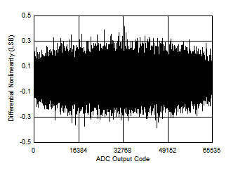
Typical DNL = ±0.4 LSB
Figure 6-3 Typical DNL
GUID-25A16270-5DCF-457D-B578-02381401C085-low.gif
 
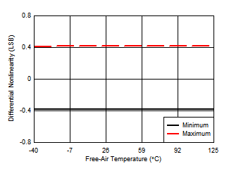
Figure 6-5 DNL vs Temperature
GUID-9D7D6667-0986-4976-BA73-B081CB846219-low.gif
 
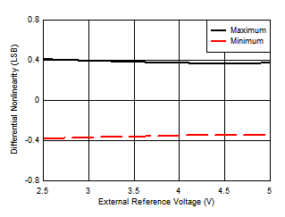
Figure 6-7 DNL vs External Reference Voltage
GUID-91F501B6-AD56-44DB-88EF-8D314BF78299-low.gif
 
Figure 6-9 Offset Error vs Temperature
GUID-D3DDA7CD-435D-4049-9910-8DD0E6FB909C-low.gif
 
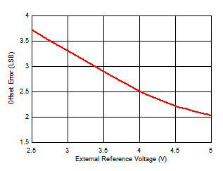
Figure 6-11 Offset Error vs External Reference Voltage
GUID-9181B62B-473E-4F3B-9FEC-1D3195D9C9FC-low.gif
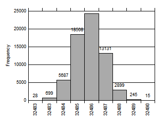
Standard deviation = 1.05 LSB
Figure 6-13 DC Input Histogram
GUID-B5AE6C19-2B3F-4D4F-94E1-F27F44D9DB9F-low.gif
 
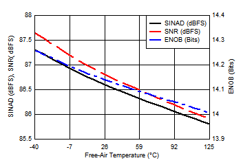
Figure 6-15 Noise Performance vs Temperature
GUID-1CB2D786-A813-42CF-88BE-B341AFE40390-low.gif
 
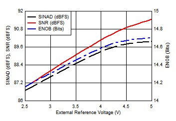
Figure 6-17 Noise Performance vs External Reference Voltage
GUID-50583EC5-8CB2-4B62-9FDB-628E72DD5962-low.gif
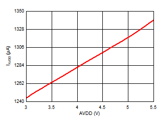
AVDD = 5 V
Figure 6-19 Analog Supply Current vs Temperature
GUID-D1321151-C1D0-4112-ACF6-A893CC2C0336-low.gif
 
Figure 6-21 Analog Supply Current vs Throughput
GUID-4B3B68BA-6DEF-4AEC-816A-4497D2735033-low.gif
Typical INL = ±1 LSB
Figure 6-4 Typical INL
GUID-0F6F6568-D71A-47A9-AB15-B33FEA0494E7-low.gif
 
Figure 6-6 INL vs Temperature
GUID-1E3CFB8F-D3D9-46E8-92B7-1E4007BED76B-low.gif
 
Figure 6-8 INL vs External Reference Voltage
GUID-83D402AB-301A-416D-9F7E-20174AF346C7-low.gif
 
Figure 6-10 Gain Error vs Temperature
GUID-47144399-1ACE-40D9-AC21-59761F821E19-low.gif
 
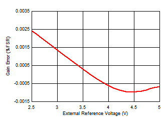
Figure 6-12 Gain Error vs External Reference Voltage
GUID-1A6B4371-8CB4-424D-B5EF-49962B9F3E4F-low.gif
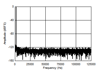
fIN = 2 kHz, SNR = 86.7 dBFS, THD = –97 dB
Figure 6-14 Typical FFT
GUID-C613C497-8763-4007-BC00-C93DB61B2C78-low.gif
 
Figure 6-16 Distortion Performance vs Temperature
GUID-7892900F-EC30-4841-A840-CFA686C236DF-low.gif
 
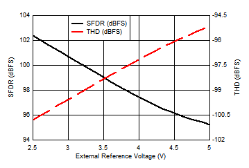
Figure 6-18 Distortion Performance vs External Reference Voltage
GUID-C3D19E62-5482-4DB7-90A6-F92DF851B83D-low.gif
TA = 25 °C
Figure 6-20 Analog Supply Current vs AVDD
GUID-20200915-CA0I-PVWT-BVNG-6TDCXLZKVNPN-low.gif
 
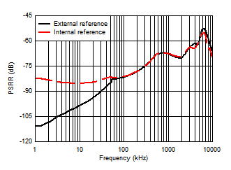
Figure 6-22 PSRR vs Frequency