ZHCSKW8C February   2020  – September 2023 ADS7066

PRODUCTION DATA  

  1.   1
  2. 特性
  3. 应用
  4. 说明
  5. Revision History
  6. Pin Configuration and Functions
  7. Specifications
    1. 6.1 Absolute Maximum Ratings
    2. 6.2 ESD Ratings
    3. 6.3 Recommended Operating Conditions
    4. 6.4 Thermal Information
    5. 6.5 Electrical Characteristics
    6. 6.6 Timing Requirements
    7. 6.7 Switching Characteristics
    8. 6.8 Timing Diagrams
    9. 6.9 Typical Characteristics
  8. Detailed Description
    1. 7.1 Overview
    2. 7.2 Functional Block Diagram
    3. 7.3 Feature Description
      1. 7.3.1  Analog Input and Multiplexer
      2. 7.3.2  Reference
        1. 7.3.2.1 External Reference
        2. 7.3.2.2 Internal Reference
      3. 7.3.3  ADC Transfer Function
      4. 7.3.4  ADC Offset Calibration
      5. 7.3.5  Programmable Averaging Filters
      6. 7.3.6  CRC on Data Interface
      7. 7.3.7  Oscillator and Timing Control
      8. 7.3.8  Diagnostic Modes
        1. 7.3.8.1 Bit-Walk Test Mode
        2. 7.3.8.2 Fixed Voltage Test Mode
      9. 7.3.9  Output Data Format
        1. 7.3.9.1 Status Flags
        2. 7.3.9.2 Output CRC (Device to Host)
        3. 7.3.9.3 Input CRC (Host to Device)
      10. 7.3.10 Device Programming
        1. 7.3.10.1 Enhanced-SPI Interface
        2. 7.3.10.2 Daisy-Chain Mode
        3. 7.3.10.3 Register Read/Write Operation
          1. 7.3.10.3.1 Register Write
          2. 7.3.10.3.2 Register Read
            1. 7.3.10.3.2.1 Register Read With CRC
    4. 7.4 Device Functional Modes
      1. 7.4.1 Device Power-Up and Reset
      2. 7.4.2 Manual Mode
      3. 7.4.3 On-the-Fly Mode
      4. 7.4.4 Auto-Sequence Mode
    5. 7.5 ADS7066 Registers
  9. Application and Implementation
    1. 8.1 Application Information
    2. 8.2 Typical Application
      1. 8.2.1 Design Requirements
      2. 8.2.2 Detailed Design Procedure
        1. 8.2.2.1 Charge-Kickback Filter and ADC Amplifier
      3. 8.2.3 Application Curve
    3. 8.3 Power Supply Recommendations
      1. 8.3.1 AVDD and DVDD Supply Recommendations
    4. 8.4 Layout
      1. 8.4.1 Layout Guidelines
      2. 8.4.2 Layout Example
  10. Device and Documentation Support
    1. 9.1 Device Support
      1. 9.1.1 Development Support
    2. 9.2 Documentation Support
      1. 9.2.1 Related Documentation
    3. 9.3 接收文档更新通知
    4. 9.4 支持资源
    5. 9.5 Trademarks
    6. 9.6 静电放电警告
    7. 9.7 术语表
  11. 10Mechanical, Packaging, and Orderable Information

封装选项

机械数据 (封装 | 引脚)
散热焊盘机械数据 (封装 | 引脚)
订购信息

Analog Input and Multiplexer

The eight channels of the multiplexer can be independently configured as ADC inputs or general-purpose inputs/outputs (GPIOs). As shown in Figure 7-1, each input pin has ESD protection diodes to AVDD and GND. On power-up or after device reset, all eight channels of the multiplexer are configured as analog inputs.
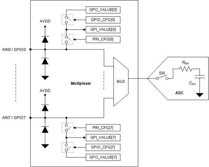
GUID-EA37A2A2-C22A-41E5-9866-678002DBA4B8-low.gif Figure 7-1 Analog Inputs, GPIOs, and ADC Connections

Figure 7-1 shows an equivalent circuit for the pins configured as analog inputs. The ADC sampling switch is represented by an ideal switch (SW) in series with a resistor (RSW, typically 150 Ω) and a sampling capacitor (CSH, typically 30 pF). During acquisition, the SW switch is closed to allow the signal on the selected analog input channel to charge the internal sampling capacitor. During conversion, the SW switch is opened to disconnect the analog input channel from the sampling capacitor.

The multiplexer channels can be configured as GPIOs in the PIN_CFG register. On power-up, all channels of the multiplexer are configured as analog inputs. The direction of a GPIO, input or output, can be set in the GPIO_CFG register. The logic level of channels configured as digital inputs can be read from the GPI_VALUE register. The digital outputs can be accessed by writing to the GPO_VALUE register. The digital outputs can be configured as open-drain or push-pull in the GPO_DRIVE_CFG register.