ZHCSLR7B March   2021  – September 2024 ADS7067

PRODUCTION DATA  

  1.   1
  2. 特性
  3. 应用
  4. 说明
  5. Pin Configuration and Functions
  6. Specifications
    1. 5.1 Absolute Maximum Ratings
    2. 5.2 ESD Ratings
    3. 5.3 Recommended Operating Conditions
    4. 5.4 Thermal Information
    5. 5.5 Electrical Characteristics
    6. 5.6 Timing Requirements
    7. 5.7 Switching Characteristics
    8. 5.8 Timing Diagrams
    9. 5.9 Typical Characteristics
  7. Detailed Description
    1. 6.1 Overview
    2. 6.2 Functional Block Diagram
    3. 6.3 Feature Description
      1. 6.3.1  Analog Input and Multiplexer
      2. 6.3.2  Reference
        1. 6.3.2.1 External Reference
        2. 6.3.2.2 Internal Reference
      3. 6.3.3  ADC Transfer Function
      4. 6.3.4  ADC Offset Calibration
      5. 6.3.5  Programmable Averaging Filters
      6. 6.3.6  CRC on Data Interface
      7. 6.3.7  Oscillator and Timing Control
      8. 6.3.8  Diagnostic Modes
        1. 6.3.8.1 Bit-Walk Test Mode
        2. 6.3.8.2 Fixed Voltage Test Mode
      9. 6.3.9  Output Data Format
        1. 6.3.9.1 Status Flags
        2. 6.3.9.2 Output CRC (Device to Host)
        3. 6.3.9.3 Input CRC (Host to Device)
      10. 6.3.10 Device Programming
        1. 6.3.10.1 Enhanced-SPI Interface
        2. 6.3.10.2 Daisy-Chain Mode
        3. 6.3.10.3 Register Read/Write Operation
          1. 6.3.10.3.1 Register Write
          2. 6.3.10.3.2 Register Read
            1. 6.3.10.3.2.1 Register Read With CRC
    4. 6.4 Device Functional Modes
      1. 6.4.1 Device Power-Up and Reset
      2. 6.4.2 Manual Mode
      3. 6.4.3 On-the-Fly Mode
      4. 6.4.4 Auto-Sequence Mode
    5. 6.5 ADS7067 Registers
  8. Application and Implementation
    1. 7.1 Application Information
    2. 7.2 Typical Application
      1. 7.2.1 Design Requirements
      2. 7.2.2 Detailed Design Procedure
        1. 7.2.2.1 Charge-Kickback Filter and ADC Amplifier
      3. 7.2.3 Application Curve
    3. 7.3 Power Supply Recommendations
      1. 7.3.1 AVDD and DVDD Supply Recommendations
    4. 7.4 Layout
      1. 7.4.1 Layout Guidelines
      2. 7.4.2 Layout Example
  9. Device and Documentation Support
    1. 8.1 Device Support
      1. 8.1.1 Development Support
    2. 8.2 Documentation Support
      1. 8.2.1 Related Documentation
    3. 8.3 接收文档更新通知
    4. 8.4 支持资源
    5. 8.5 Trademarks
    6. 8.6 静电放电警告
    7. 8.7 术语表
  10. Revision History
  11. 10Mechanical, Packaging, and Orderable Information

封装选项

机械数据 (封装 | 引脚)
散热焊盘机械数据 (封装 | 引脚)
订购信息

Manual Mode

Manual mode allows the external host processor to directly select the analog input channel. Figure 6-12 shows steps for operating the device in manual mode.

ADS7067 Device Operation in Manual
          Mode Figure 6-12 Device Operation in Manual Mode

In manual mode, the command to switch to a new channel, cycle N in Figure 6-13, is decoded by the device on the CS rising edge. The CS rising edge is also the start of the conversion cycle, and thus the device samples the previously selected MUX channel in cycle N+1. The newly selected analog input channel data are available in cycle N+2. For switching the analog input channel, a register write to the MANUAL_CHID field requires 24 clocks; see the Register Write section for more details. After a channel is selected, the number of clocks required for reading the output data depends on the device output data frame size; see the Output Data Format section for more details.
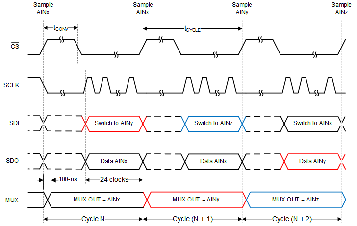
ADS7067 Starting a Conversion and Reading Data in Manual ModeFigure 6-13 Starting a Conversion and Reading Data in Manual Mode