ZHCSJ06B November 2017 – September 2022 ADS7142-Q1
PRODUCTION DATA
- 1 特性
- 2 应用
- 3 说明
- 4 Revision History
- 5 Pin Configuration and Functions
-
6 Specifications
- 6.1 Absolute Maximum Ratings
- 6.2 ESD Ratings
- 6.3 Recommended Operating Conditions
- 6.4 Thermal Information
- 6.5 Electrical Characteristics: All Modes
- 6.6 Electrical Characteristics: Manual Mode
- 6.7 Electrical Characteristics: Autonomous Modes
- 6.8 Electrical Characteristics: High Precision Mode
- 6.9 Timing Requirements
- 6.10 Switching Characteristics
- 6.11 Timing Diagrams
- 6.12 Typical Characteristics: All Modes
- 6.13 Typical Characteristics: Manual Mode
- 6.14 Typical Characteristics: Autonomous Modes
- 6.15 Typical Characteristics: High-Precision Mode
-
7 Detailed Description
- 7.1 Overview
- 7.2 Functional Block Diagram
- 7.3 Feature Description
- 7.4 Device Functional Modes
- 7.5 Programming
- 7.6 Register Map
- 8 Application and Implementation
- 9 Device and Documentation Support
- 10Mechanical, Packaging, and Orderable Information
8.2.1.2.1 Programmable Thresholds and Hysteresis
The ADS7142-Q1 can be programmed to monitor sensor output voltages and generate an ALERT signal to the host controller if the sensor output voltage crosses a threshold.
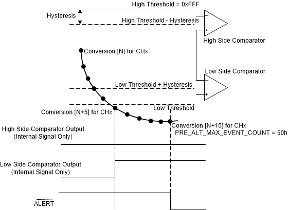
The device can be configured to monitor for signals rising above a programmed threshold. Figure 8-3 illustrates the operation of the device when monitoring for signal crossings on the low threshold by setting the high threshold to 0xFFF. In this case, the output of the low-side comparator is set whenever the ADC conversion result is less than or equal to the low threshold, and the output of the high-side comparator is only set when the ADC conversion result is equal to 0xFFF.
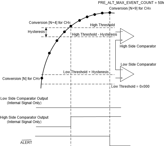
The device can also be configured to monitor for signals falling below a programmed threshold. Figure 8-4 illustrates the operation of the device when monitoring for signal crossings on the high threshold by setting the low threshold to 0x000. In this case, the output of high-side comparator is set whenever the ADC conversion result is greater than or equal to the high threshold and the output of the low-side comparator is only set when the ADC conversion result is equal to 0x000.
 Figure 8-3 Low Alert
With the ADS7142-Q1
 Figure 8-4 High
Alert With the ADS7142-Q1
Figure 8-4 High
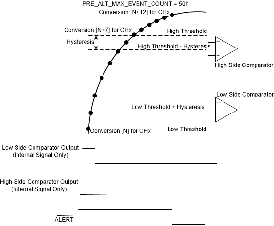
Alert With the ADS7142-Q1The device can also be configured to monitor for signals falling outside of a programmed window. Figure 8-5 shows the device operation for an out-of-range alert where the signal leaves the predefined window and crosses either the high or low threshold. In this case, the output of the low-side comparator is set whenever the ADC conversion result is less than or equal to the low threshold, and the output of the high-side comparator is set when the ADC conversion result is greater than or equal to the high threshold.
 Figure 8-5 Out of Range Alert With
the ADS7142-Q1