ZHCSH75A September   2017  – December 2017 ADS7142

PRODUCTION DATA.  

  1. 特性
  2. 应用
  3. 说明
    1.     Device Images
  4. 修订历史记录
  5. Pin Configuration and Functions
    1.     Pin Functions
  6. Specifications
    1. 6.1  Absolute Maximum Ratings
    2. 6.2  ESD Ratings
    3. 6.3  Recommended Operating Conditions
    4. 6.4  Thermal Information
    5. 6.5  Electrical Characteristics - All Modes
    6. 6.6  Electrical Characteristics - Manual Mode
    7. 6.7  Electrical Characteristics - Autonomous Modes
    8. 6.8  Electrical Characteristics - High Precision Mode
    9. 6.9  Timing Requirements
    10. 6.10 Switching Characteristics
    11. 6.11 Typical Characteristics for All Modes
    12. 6.12 Typical Characteristics for Manual Mode
    13. 6.13 Typical Characteristics for Autonomous Modes
    14. 6.14 Typical Characteristics for High Precision Mode
  7. Detailed Description
    1. 7.1 Overview
    2. 7.2 Functional Block Diagram
    3. 7.3 Feature Description
      1. 7.3.1  Analog Input and Multiplexer
        1. 7.3.1.1 Two-Channel, Single-Ended Configuration
        2. 7.3.1.2 Single-Channel, Single-Ended Configuration
        3. 7.3.1.3 Single-Channel, Pseudo-Differential Configuration
      2. 7.3.2  OFFSET Calibration
      3. 7.3.3  Reference
      4. 7.3.4  ADC Transfer Function
      5. 7.3.5  Oscillator and Timing Control
      6. 7.3.6  I2C Address Selector
      7. 7.3.7  Data Buffer
        1. 7.3.7.1 Filling of the Data Buffer
        2. 7.3.7.2 Reading data from the Data Buffer
      8. 7.3.8  Accumulator
      9. 7.3.9  Digital Window Comparator
      10. 7.3.10 I2C Protocol Features
        1. 7.3.10.1 General Call
        2. 7.3.10.2 General Call with Software Reset
        3. 7.3.10.3 General Call with Write Software programmable part of slave address
        4. 7.3.10.4 Configuring Device into High Speed I2C mode
        5. 7.3.10.5 Bus Clear
      11. 7.3.11 Device Programming
        1. 7.3.11.1 Reading Registers
          1. 7.3.11.1.1 Single Register Read
          2. 7.3.11.1.2 Reading a Continuous Block of Registers
        2. 7.3.11.2 Writing Registers
          1. 7.3.11.2.1 Single Register Write
          2. 7.3.11.2.2 Set Bit
          3. 7.3.11.2.3 Clear Bit
          4. 7.3.11.2.4 Writing a continuous block of registers
    4. 7.4 Device Functional Modes
      1. 7.4.1 Device Power Up and Reset
      2. 7.4.2 Manual Mode
        1. 7.4.2.1 Manual Mode with CH0 Only
        2. 7.4.2.2 Manual Mode with AUTO Sequence
      3. 7.4.3 Autonomous Modes
        1. 7.4.3.1 Autonomous Mode with Threshold Monitoring and Diagnostics
          1. 7.4.3.1.1 Autonomous Mode with Pre Alert Data
          2. 7.4.3.1.2 Autonomous Mode with Post Alert Data
        2. 7.4.3.2 Autonomous Mode with Burst Data
          1. 7.4.3.2.1 Autonomous Mode with Start Burst
          2. 7.4.3.2.2 Autonomous Mode with Stop Burst
      4. 7.4.4 High Precision Mode
    5. 7.5 Optimizing Power Consumed by the Device
    6. 7.6 Register Map
      1. 7.6.1 RESET REGISTERS
        1. 7.6.1.1 WKEY Register (address = 17h), [reset = 00h]
          1. Table 6. WKEY Register Field Descriptions
        2. 7.6.1.2 DEVICE_RESET Register (address = 14h), [reset = 00h]
          1. Table 7. DEVICE_RESET Register Field Descriptions
      2. 7.6.2 FUNCTIONAL MODE SELECT REGISTERS
        1. 7.6.2.1 OFFSET_CAL Register (address = 15h), [reset = 00h]
          1. Table 8. OFFSET_CAL Register Field Descriptions
        2. 7.6.2.2 OPMODE_SEL Register (address = 1Ch), [reset = 00h]
          1. Table 9. OPMODE_SEL Register Field Descriptions
        3. 7.6.2.3 OPMODE_I2CMODE_STATUS Register (address = 00h), [reset = 00h]
          1. Table 10. OPMODE_I2CMODE_STATUS Register Field Descriptions
      3. 7.6.3 INPUT CONFIG REGISTER
        1. 7.6.3.1 CHANNEL_INPUT_CFG Register (address = 24h), [reset = 00h]
          1. Table 11. CHANNEL_INPUT_CFG Register Field Descriptions
      4. 7.6.4 ANALOG MUX and SEQUENCER REGISTERS
        1. 7.6.4.1 AUTO_SEQ_CHEN Register (address = 20h), [reset = 03h]
          1. Table 12. AUTO_SEQ_CHEN Register Field Descriptions
        2. 7.6.4.2 START_SEQUENCE Register (address = 1Eh), [reset = 00h]
          1. Table 13. START_SEQUENCE Register Field Descriptions
        3. 7.6.4.3 ABORT_SEQUENCE Register (address = 1Fh), [reset = 00h]
          1. Table 14. ABORT_SEQUENCE Register Field Descriptions
        4. 7.6.4.4 SEQUENCE_STATUS Register (address = 04h), [reset = 00h]
          1. Table 15. SEQUENCE_STATUS Register Field Descriptions
      5. 7.6.5 OSCILLATOR and TIMING CONTROL REGISTERS
        1. 7.6.5.1 OSC_SEL Register (address = 18h), [reset = 00h]
          1. Table 16. OSC_SEL Register Field Descriptions
        2. 7.6.5.2 nCLK_SEL Register (address = 19h), [reset = 00h]
          1. Table 17. nCLK_SEL Register Field Descriptions
      6. 7.6.6 DATA BUFFER CONTROL REGISTER
        1. 7.6.6.1 DATA_BUFFER_OPMODE Register (address = 2Ch), [reset = 01h]
          1. Table 18. DATA_BUFFER_OPMODE Register Field Descriptions
        2. 7.6.6.2 DOUT_FORMAT_CFG Register (address = 28h), [reset = 00h]
          1. Table 19. DOUT_FORMAT_CFG Register Field Descriptions
        3. 7.6.6.3 DATA_BUFFER_STATUS Register (address = 01h), [reset = 00h]
          1. Table 20. DATA_BUFFER_STATUS Register Field Descriptions
      7. 7.6.7 ACCUMULATOR CONTROL REGISTERS
        1. 7.6.7.1 ACC_EN Register (address = 30h), [reset = 00h]
          1. Table 21. ACC_EN Register Field Descriptions
        2. 7.6.7.2 ACC_CH0_LSB Register (address = 08h), [reset = 00h]
          1. Table 22. ACC_CH0_LSB Register Field Descriptions
        3. 7.6.7.3 ACC_CH0_MSB Register (address = 09h), [reset = 00h]
          1. Table 23. ACC_CH0_MSB Register Field Descriptions
        4. 7.6.7.4 ACC_CH1_LSB Register (address = 0Ah), [reset = 00h]
          1. Table 24. ACC_CH1 LSB Register Field Descriptions
        5. 7.6.7.5 ACC_CH1_MSB Register (address = 0Bh), [reset = 00h]
          1. Table 25. ACC_CH1 MSB Register Field Descriptions
        6. 7.6.7.6 ACCUMULATOR_STATUS Register (address = 02h), [reset = 00h]
          1. Table 26. ACCUMULATOR_STATUS Register Field Descriptions
      8. 7.6.8 DIGITAL WINDOW COMPARATOR REGISTERS
        1. 7.6.8.1  ALERT_DWC_EN Register (address = 37h), [reset = 00h]
          1. Table 27. ALERT_DWC_EN Register Field Descriptions
        2. 7.6.8.2  ALERT_CHEN (address = 34h), [reset = 00h]
          1. Table 28. ALERT_CHEN Register Field Descriptions
        3. 7.6.8.3  DWC_HTH_CH0_MSB Register (address = 39h), [reset = 00h]
          1. Table 29. DWC_HTH_CH0_LSB Register Field Descriptions
        4. 7.6.8.4  DWC_HTH_CH0_LSB Register (address = 38h), [reset = 00h]
          1. Table 30. DWC_HTH_CH0_LSB Register Field Descriptions
        5. 7.6.8.5  DWC_LTH_CH0_MSB Register (address = 3Bh), [reset = 00h]
          1. Table 31. DWC_LTH_CH0_MSB Register Field Descriptions
        6. 7.6.8.6  DWC_LTH_CH0_LSB Register (address = 3Ah), [reset = 00h]
          1. Table 32. DWC_LTH_CH0_LSB Register Field Descriptions
        7. 7.6.8.7  DWC_HYS_CH0 (address = 40h), [reset = 00h]
          1. Table 33. DWC_HYS_CH0 Register Field Descriptions
        8. 7.6.8.8  DWC_HTH_CH1_MSB Register (address = 3Dh), [reset = 00h]
          1. Table 34. DWC_HTH_CH1_LSB Register Field Descriptions
        9. 7.6.8.9  DWC_HTH_CH1_LSB Register (address = 3Ch), [reset = 00h]
          1. Table 35. DWC_HTH_CH1_LSB Register Field Descriptions
        10. 7.6.8.10 DWC_LTH_CH1_MSB Register (address = 3Fh), [reset = 00h]
          1. Table 36. DWC_LTH_CH1_MSB Register Field Descriptions
        11. 7.6.8.11 DWC_LTH_CH1_LSB Register (address = 3Eh), [reset = 00h]
          1. Table 37. DWC_LTH_CH1_LSB Register Field Descriptions
        12. 7.6.8.12 DWC_HYS_CH1 (address = 41h), [reset = 00h]
          1. Table 38. DWC_HYS_CH1 Register Field Descriptions
        13. 7.6.8.13 PRE_ALT_MAX_EVENT_COUNT Register (address = 36h), [reset = 00h]
          1. Table 39. PRE_ALT_MAX_EVENT_COUNT Register Field Descriptions
        14. 7.6.8.14 ALERT_TRIG_CHID Register (address = 03h), [reset = 00h]
          1. Table 40. ALERT_TRIG_CHID Register Field Descriptions
        15. 7.6.8.15 ALERT_LOW_FLAGS Register (address = 0C), [reset = 00h]
          1. Table 41. ALERT_LOW_FLAGS Register Field Descriptions
        16. 7.6.8.16 ALERT_HIGH_FLAGS Register (address = 0Eh), [reset = 00h]
          1. Table 42. ALERT_HIGH_FLAGS Register Field Descriptions
  8. Application and Implementation
    1. 8.1 Application Information
    2. 8.2 Typical Applications
      1. 8.2.1 ADS7142 as a Programmable Comparator with False Trigger Prevention and Diagnostics
        1. 8.2.1.1 Design Requirements
          1. 8.2.1.1.1 Higher Power Consumption
          2. 8.2.1.1.2 Fixed Threshold Voltages
        2. 8.2.1.2 Detailed Design Procedure
          1. 8.2.1.2.1 Programmable Thresholds and Hysteresis
          2. 8.2.1.2.2 False Trigger Prevention with Event Counter
          3. 8.2.1.2.3 Fault Diagnostics with Data Buffer
        3. 8.2.1.3 Application Curve
      2. 8.2.2 Event-triggered PIR sensing with ADS7142
        1. 8.2.2.1 Design Requirements
        2. 8.2.2.2 Detailed Design Procedure
        3. 8.2.2.3 Application Curves
  9. Power-Supply Recommendations
    1. 9.1 AVDD and DVDD Supply Recommendations
  10. 10Layout
    1. 10.1 Layout Guidelines
    2. 10.2 Layout Example
  11. 11器件和文档支持
    1. 11.1 文档支持
    2. 11.2 接收文档更新通知
    3. 11.3 社区资源
    4. 11.4 商标
    5. 11.5 静电放电警告
    6. 11.6 Glossary
  12. 12机械、封装和可订购信息

封装选项

机械数据 (封装 | 引脚)
散热焊盘机械数据 (封装 | 引脚)
订购信息

Programmable Thresholds and Hysteresis

The ADS7142 can be programmed to monitor sensor output voltages and generate an ALERT signal for the host controller if the sensor output voltage crosses a threshold.

The device can be configured to monitor for signals rising above a programmed threshold. Figure 114 illustrates the operation of the device when monitoring for signal crossings on the low threshold by setting the high threshold to 0xFFF. In this example, the output of the low-side comparator is set whenever the ADC conversion result is less than or equal to the low threshold, and the output of the high-side comparator is only set when the ADC conversion result is equal to 0xFFF.

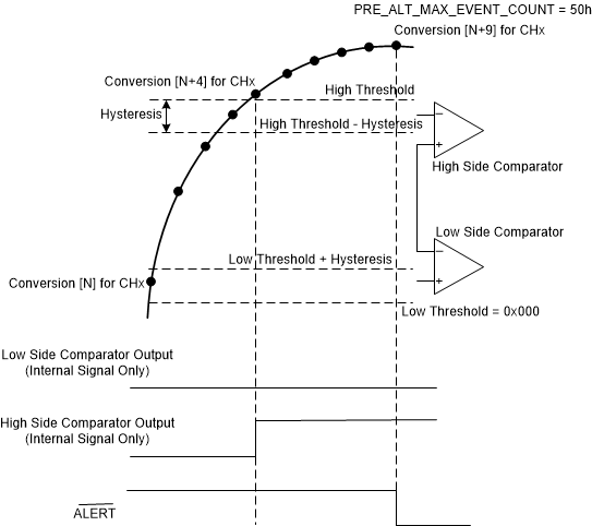
The device can also be configured to monitor for signals falling below a programmed threshold. Figure 115 illustrates the operation of the device when monitoring for signal crossings on the high threshold by setting the low threshold to 0x000. In this example, the output of high-side comparator is set whenever the ADC conversion result is greater than or equal to the high threshold and the output of the low-side comparator is only set when the ADC conversion result is equal to 0x000.
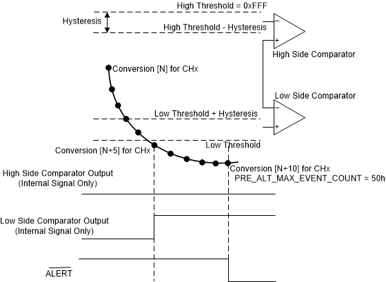
ADS7142 low_alert_sbas773.gifFigure 114. Low Alert with ADS7142
ADS7142 high_alert_sbas773.gifFigure 115. High Alert with ADS7142

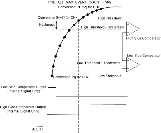
The device can also be configured to monitor for signals falling outside of a programmed window. Figure 116 illustrates the operation of the device for an out-of-range alert where the signal leaves the pre-defined window and crosses either the high or low threshold. In this example, the output of low side comparator is set whenever the ADC conversion result is less than or equal to the low threshold, and the output of high side comparator is set when the ADC conversion result is greater than or equal to the high threshold.
ADS7142 out_of_range_alert_sbas773.gifFigure 116. Out of Range Alert with ADS7142