ZHCSH75A
September 2017 – December 2017
ADS7142
PRODUCTION DATA.
1
特性
2
应用
3
说明
Device Images
4
修订历史记录
5
Pin Configuration and Functions
Pin Functions
6
Specifications
6.1
Absolute Maximum Ratings
6.2
ESD Ratings
6.3
Recommended Operating Conditions
6.4
Thermal Information
6.5
Electrical Characteristics - All Modes
6.6
Electrical Characteristics - Manual Mode
6.7
Electrical Characteristics - Autonomous Modes
6.8
Electrical Characteristics - High Precision Mode
6.9
Timing Requirements
6.10
Switching Characteristics
6.11
Typical Characteristics for All Modes
6.12
Typical Characteristics for Manual Mode
6.13
Typical Characteristics for Autonomous Modes
6.14
Typical Characteristics for High Precision Mode
7
Detailed Description
7.1
Overview
7.2
Functional Block Diagram
7.3
Feature Description
7.3.1
Analog Input and Multiplexer
7.3.1.1
Two-Channel, Single-Ended Configuration
7.3.1.2
Single-Channel, Single-Ended Configuration
7.3.1.3
Single-Channel, Pseudo-Differential Configuration
7.3.2
OFFSET Calibration
7.3.3
Reference
7.3.4
ADC Transfer Function
7.3.5
Oscillator and Timing Control
7.3.6
I2C Address Selector
7.3.7
Data Buffer
7.3.7.1
Filling of the Data Buffer
7.3.7.2
Reading data from the Data Buffer
7.3.8
Accumulator
7.3.9
Digital Window Comparator
7.3.10
I2C Protocol Features
7.3.10.1
General Call
7.3.10.2
General Call with Software Reset
7.3.10.3
General Call with Write Software programmable part of slave address
7.3.10.4
Configuring Device into High Speed I2C mode
7.3.10.5
Bus Clear
7.3.11
Device Programming
7.3.11.1
Reading Registers
7.3.11.1.1
Single Register Read
7.3.11.1.2
Reading a Continuous Block of Registers
7.3.11.2
Writing Registers
7.3.11.2.1
Single Register Write
7.3.11.2.2
Set Bit
7.3.11.2.3
Clear Bit
7.3.11.2.4
Writing a continuous block of registers
7.4
Device Functional Modes
7.4.1
Device Power Up and Reset
7.4.2
Manual Mode
7.4.2.1
Manual Mode with CH0 Only
7.4.2.2
Manual Mode with AUTO Sequence
7.4.3
Autonomous Modes
7.4.3.1
Autonomous Mode with Threshold Monitoring and Diagnostics
7.4.3.1.1
Autonomous Mode with Pre Alert Data
7.4.3.1.2
Autonomous Mode with Post Alert Data
7.4.3.2
Autonomous Mode with Burst Data
7.4.3.2.1
Autonomous Mode with Start Burst
7.4.3.2.2
Autonomous Mode with Stop Burst
7.4.4
High Precision Mode
7.5
Optimizing Power Consumed by the Device
7.6
Register Map
7.6.1
RESET REGISTERS
7.6.1.1
WKEY Register (address = 17h), [reset = 00h]
Table 6.
WKEY Register Field Descriptions
7.6.1.2
DEVICE_RESET Register (address = 14h), [reset = 00h]
Table 7.
DEVICE_RESET Register Field Descriptions
7.6.2
FUNCTIONAL MODE SELECT REGISTERS
7.6.2.1
OFFSET_CAL Register (address = 15h), [reset = 00h]
Table 8.
OFFSET_CAL Register Field Descriptions
7.6.2.2
OPMODE_SEL Register (address = 1Ch), [reset = 00h]
Table 9.
OPMODE_SEL Register Field Descriptions
7.6.2.3
OPMODE_I2CMODE_STATUS Register (address = 00h), [reset = 00h]
Table 10.
OPMODE_I2CMODE_STATUS Register Field Descriptions
7.6.3
INPUT CONFIG REGISTER
7.6.3.1
CHANNEL_INPUT_CFG Register (address = 24h), [reset = 00h]
Table 11.
CHANNEL_INPUT_CFG Register Field Descriptions
7.6.4
ANALOG MUX and SEQUENCER REGISTERS
7.6.4.1
AUTO_SEQ_CHEN Register (address = 20h), [reset = 03h]
Table 12.
AUTO_SEQ_CHEN Register Field Descriptions
7.6.4.2
START_SEQUENCE Register (address = 1Eh), [reset = 00h]
Table 13.
START_SEQUENCE Register Field Descriptions
7.6.4.3
ABORT_SEQUENCE Register (address = 1Fh), [reset = 00h]
Table 14.
ABORT_SEQUENCE Register Field Descriptions
7.6.4.4
SEQUENCE_STATUS Register (address = 04h), [reset = 00h]
Table 15.
SEQUENCE_STATUS Register Field Descriptions
7.6.5
OSCILLATOR and TIMING CONTROL REGISTERS
7.6.5.1
OSC_SEL Register (address = 18h), [reset = 00h]
Table 16.
OSC_SEL Register Field Descriptions
7.6.5.2
nCLK_SEL Register (address = 19h), [reset = 00h]
Table 17.
nCLK_SEL Register Field Descriptions
7.6.6
DATA BUFFER CONTROL REGISTER
7.6.6.1
DATA_BUFFER_OPMODE Register (address = 2Ch), [reset = 01h]
Table 18.
DATA_BUFFER_OPMODE Register Field Descriptions
7.6.6.2
DOUT_FORMAT_CFG Register (address = 28h), [reset = 00h]
Table 19.
DOUT_FORMAT_CFG Register Field Descriptions
7.6.6.3
DATA_BUFFER_STATUS Register (address = 01h), [reset = 00h]
Table 20.
DATA_BUFFER_STATUS Register Field Descriptions
7.6.7
ACCUMULATOR CONTROL REGISTERS
7.6.7.1
ACC_EN Register (address = 30h), [reset = 00h]
Table 21.
ACC_EN Register Field Descriptions
7.6.7.2
ACC_CH0_LSB Register (address = 08h), [reset = 00h]
Table 22.
ACC_CH0_LSB Register Field Descriptions
7.6.7.3
ACC_CH0_MSB Register (address = 09h), [reset = 00h]
Table 23.
ACC_CH0_MSB Register Field Descriptions
7.6.7.4
ACC_CH1_LSB Register (address = 0Ah), [reset = 00h]
Table 24.
ACC_CH1 LSB Register Field Descriptions
7.6.7.5
ACC_CH1_MSB Register (address = 0Bh), [reset = 00h]
Table 25.
ACC_CH1 MSB Register Field Descriptions
7.6.7.6
ACCUMULATOR_STATUS Register (address = 02h), [reset = 00h]
Table 26.
ACCUMULATOR_STATUS Register Field Descriptions
7.6.8
DIGITAL WINDOW COMPARATOR REGISTERS
7.6.8.1
ALERT_DWC_EN Register (address = 37h), [reset = 00h]
Table 27.
ALERT_DWC_EN Register Field Descriptions
7.6.8.2
ALERT_CHEN (address = 34h), [reset = 00h]
Table 28.
ALERT_CHEN Register Field Descriptions
7.6.8.3
DWC_HTH_CH0_MSB Register (address = 39h), [reset = 00h]
Table 29.
DWC_HTH_CH0_LSB Register Field Descriptions
7.6.8.4
DWC_HTH_CH0_LSB Register (address = 38h), [reset = 00h]
Table 30.
DWC_HTH_CH0_LSB Register Field Descriptions
7.6.8.5
DWC_LTH_CH0_MSB Register (address = 3Bh), [reset = 00h]
Table 31.
DWC_LTH_CH0_MSB Register Field Descriptions
7.6.8.6
DWC_LTH_CH0_LSB Register (address = 3Ah), [reset = 00h]
Table 32.
DWC_LTH_CH0_LSB Register Field Descriptions
7.6.8.7
DWC_HYS_CH0 (address = 40h), [reset = 00h]
Table 33.
DWC_HYS_CH0 Register Field Descriptions
7.6.8.8
DWC_HTH_CH1_MSB Register (address = 3Dh), [reset = 00h]
Table 34.
DWC_HTH_CH1_LSB Register Field Descriptions
7.6.8.9
DWC_HTH_CH1_LSB Register (address = 3Ch), [reset = 00h]
Table 35.
DWC_HTH_CH1_LSB Register Field Descriptions
7.6.8.10
DWC_LTH_CH1_MSB Register (address = 3Fh), [reset = 00h]
Table 36.
DWC_LTH_CH1_MSB Register Field Descriptions
7.6.8.11
DWC_LTH_CH1_LSB Register (address = 3Eh), [reset = 00h]
Table 37.
DWC_LTH_CH1_LSB Register Field Descriptions
7.6.8.12
DWC_HYS_CH1 (address = 41h), [reset = 00h]
Table 38.
DWC_HYS_CH1 Register Field Descriptions
7.6.8.13
PRE_ALT_MAX_EVENT_COUNT Register (address = 36h), [reset = 00h]
Table 39.
PRE_ALT_MAX_EVENT_COUNT Register Field Descriptions
7.6.8.14
ALERT_TRIG_CHID Register (address = 03h), [reset = 00h]
Table 40.
ALERT_TRIG_CHID Register Field Descriptions
7.6.8.15
ALERT_LOW_FLAGS Register (address = 0C), [reset = 00h]
Table 41.
ALERT_LOW_FLAGS Register Field Descriptions
7.6.8.16
ALERT_HIGH_FLAGS Register (address = 0Eh), [reset = 00h]
Table 42.
ALERT_HIGH_FLAGS Register Field Descriptions
8
Application and Implementation
8.1
Application Information
8.2
Typical Applications
8.2.1
ADS7142 as a Programmable Comparator with False Trigger Prevention and Diagnostics
8.2.1.1
Design Requirements
8.2.1.1.1
Higher Power Consumption
8.2.1.1.2
Fixed Threshold Voltages
8.2.1.2
Detailed Design Procedure
8.2.1.2.1
Programmable Thresholds and Hysteresis
8.2.1.2.2
False Trigger Prevention with Event Counter
8.2.1.2.3
Fault Diagnostics with Data Buffer
8.2.1.3
Application Curve
8.2.2
Event-triggered PIR sensing with ADS7142
8.2.2.1
Design Requirements
8.2.2.2
Detailed Design Procedure
8.2.2.3
Application Curves
9
Power-Supply Recommendations
9.1
AVDD and DVDD Supply Recommendations
10
Layout
10.1
Layout Guidelines
10.2
Layout Example
11
器件和文档支持
11.1
文档支持
11.2
接收文档更新通知
11.3
社区资源
11.4
商标
11.5
静电放电警告
11.6
Glossary
12
机械、封装和可订购信息
封装选项
机械数据 (封装 | 引脚)
RUG|10
MPQF216A
散热焊盘机械数据 (封装 | 引脚)
订购信息
zhcsh75a_oa
zhcsh75a_pm
6.14
Typical Characteristics for High Precision Mode
At T
A
= 25°C, AVDD = 3 V, DVDD = 3.3 V, and Two-Channel, Single-Ended Configuration, unless otherwise noted.
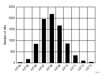
Standard Deviation = 1.49
Mean = 32768.5
Figure 34.
Typical DC Code Spread in High Precision Mode
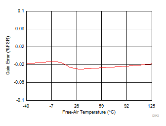
Figure 36.
Gain Error in High Precision Mode with Temperature
With High Speed Oscillator
nCLK = 25
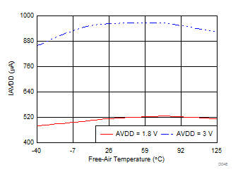
Figure 38.
I
AVDD
in High Precision Mode with Temperature
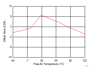
Figure 35.
Offset Error in High Precision Mode with Temperature
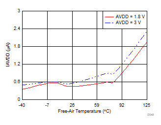
With Low Power Oscillator
nCLK = 25
Figure 37.
I
AVDD
in High Precision Mode with Temperature
千亿体育app官网登录(中国)官方网站IOS/安卓通用版/手机APP
|
米乐app下载官网(中国)|ios|Android/通用版APP最新版
|
米乐|米乐·M6(中国大陆)官方网站
|
千亿体育登陆地址
|
华体会体育(中国)HTH·官方网站
|
千赢qy国际_全站最新版千赢qy国际V6.2.14安卓/IOS下载
|
18新利网v1.2.5|中国官方网站
|
bob电竞真人(中国官网)安卓/ios苹果/电脑版【1.97.95版下载】
|
千亿体育app官方下载(中国)官方网站IOS/安卓/手机APP下载安装
|