SBAS456B December 2008 – January 2016 ADS7828-Q1
PRODUCTION DATA.
- 1 Features
- 2 Applications
- 3 Description
- 4 Revision History
- 5 Pin Configuration and Functions
-
6 Specifications
- 6.1 Absolute Maximum Ratings
- 6.2 ESD Ratings
- 6.3 Recommended Operating Conditions
- 6.4 Thermal Information
- 6.5 Electrical Characteristics for ADS7828E
- 6.6 Electrical Characteristics for ADS7828EB
- 6.7 Electrical Characteristics for ADS7828E
- 6.8 Electrical Characteristics for ADS7828EB
- 6.9 Switching Characteristics
- 6.10 Typical Characteristics
- 7 Detailed Description
- 8 Application and Implementation
- 9 Power Supply Recommendations
- 10Layout
- 11Device and Documentation Support
- 12Mechanical, Packaging, and Orderable Information
8 Application and Implementation
NOTE
Information in the following applications sections is not part of the TI component specification, and TI does not warrant its accuracy or completeness. TI’s customers are responsible for determining suitability of components for their purposes. Customers should validate and test their design implementation to confirm system functionality.
8.1 Application Information
The following sections give example circuits and suggestions for using the ADS7828-Q1 device in various situations.
8.1.1 Basic Connections
For many applications, connecting the ADS7828-Q1 device is simple. Figure 21 shows a basic connection diagram for the ADS7828-Q1 device.
The fully differential voltage input of the ADS7828-Q1 device is ideal for connection to differential sources with moderately low source impedance, such as thermocouples and thermistors. Although the ADS7828-Q1 device can read bipolar differential signals, they cannot accept negative voltages on either input. It may be helpful to think of the ADS7828-Q1 positive voltage input as noninverting, and of the negative input as inverting.
When the ADS7828-Q1 device converts data, it draws current in short spikes. The 0.1-μF bypass capacitor supplies the momentary bursts of extra current needed from the supply.
The ADS7828-Q1 device interfaces directly to standard mode, fast mode, and high-speed mode I2C controllers. Any microcontroller I2C peripheral, including master-only and non-multiple-master I2C peripherals, can operate with the ADS7828-Q1 device. The ADS7828-Q1 device does not perform clock-stretching (that is, it never pulls the clock line low), so it is not necessary to provide for this function unless other clock-stretching devices are on the same I2C bus.
Pullup resistors are required on both the SDA and SCL lines because I2C bus drivers are open-drain. The size of these resistors depends on the bus operating speed and capacitance of the bus lines. Higher-value resistors consume less power, but increase the transition times on the bus, limiting the bus speed. Lower-value resistors allow higher speed at the expense of higher power consumption. Long bus lines have higher capacitance and require smaller pullup resistors to compensate. The resistors should not be too small; if they are, the bus drivers may not be able to pull the bus lines low.
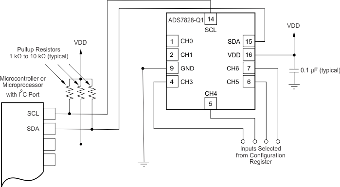 Figure 21. Typical Connections of the ADS7828-Q1
8.1.1.1 Connecting Multiple Devices
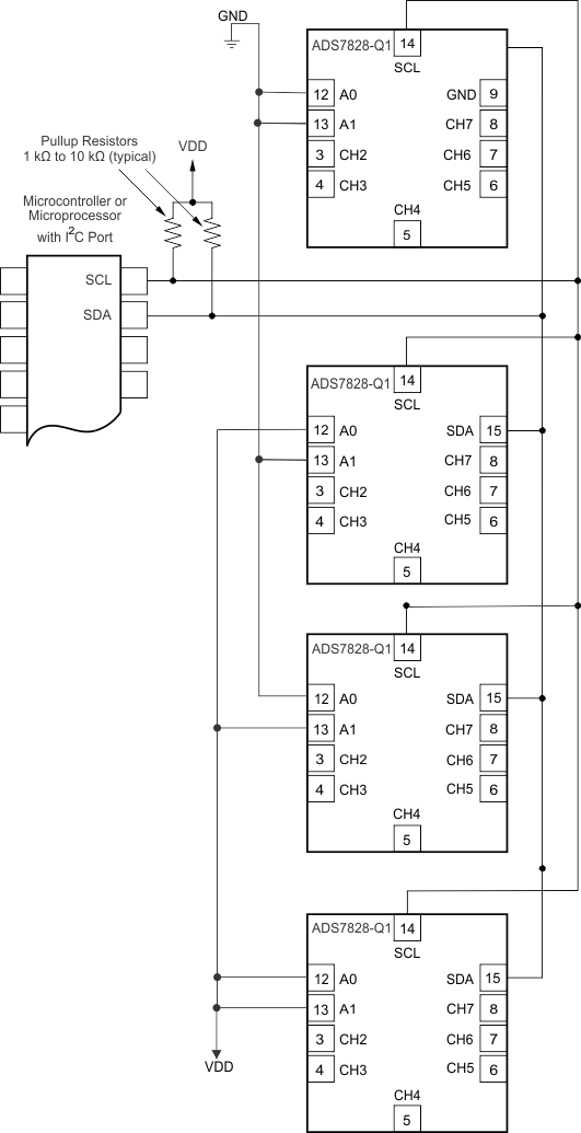
Connecting multiple ADS7828-Q1 devices to a single bus is simple. Using the address pin, the ADS7828-Q1 device can be set to one of four different I2C addresses. Figure 22 shows an example using three ADS7828-Q1 devices. Up to four ADS7828-Q1 devices (using different address pin configurations) can be connected to a single bus.
Only one set of pullup resistors is require per bus. The pullup resistor values can be lowered slightly to compensate for the additional bus capacitance presented by multiple devices and increased line length.
8.1.1.2 Using GPIO Ports for Communication
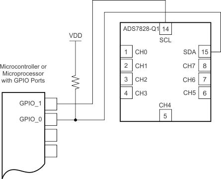
Most microcontrollers have programmable input-output (I/O) pins that can be set in software to act as inputs or outputs. If an I2C controller is not available, the ADS7828-Q1 device can be connected to GPIO pins and the I2C bus protocol simulated, or bit-banged, in software. Figure 23 shows an example of this configuration for a single ADS7828-Q1 device.
Bit-banging the I2C with GPIO pins occurs by setting the GPIO line to 0 and toggling it between input and output modes to apply the proper bus states. To drive the line low, the pin is set to output 0; to let the line go high, the pin is set to input. When the pin is set to input, the state of the pin can be read; if another device is pulling the line low, this configuration reads as a 0 in the port input register.
Note that no pullup resistor is shown on the SCL line. In this simple case, the resistor is not needed; the microcontroller can simply leave the line on output, and set it to 1 or 0 as appropriate. This action is possible because the ADS7828-Q1 never drives the clock line low. This technique can also be used with multiple devices, and has the advantage of lower current consumption as a result of the absence of a resistive pullup.
If there are any devices on the bus that may drive the clock lines low, this method should not be used; the SCL line should be high-Z or 0 and a pullup resistor provided as usual.
Some microcontrollers have selectable strong pullup circuits built into the GPIO ports. In some cases, these circuits can be switched on and used in place of an external pullup resistor. Weak pullups are also provided on some microcontrollers, but usually these are too weak for I2C communication. If there is any doubt about the matter, test the circuit before committing it to production.
8.1.1.3 Single-Ended Inputs
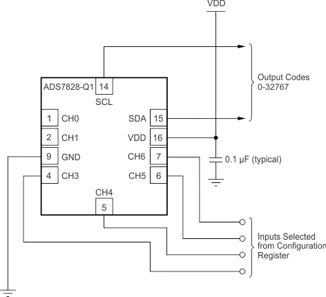
Although the ADS7828-Q1 device has four differential inputs, the device can easily measure eight single-ended signals. Figure 24 shows a single-ended connection scheme. The ADS7828-Q1 device is configured for single-ended measurement by configuring the MUX to measure each channel with respect to ground. Data are then read out of one input based on the selection on the configuration register. The single-ended signal can range from 0 V to the supply voltage. The ADS7828-Q1 device loses no linearity anywhere within the input range. Negative voltages cannot be applied to this circuit because the ADS7828-Q1 device can only accept positive voltages.
The ADS7828-Q1 input range is bipolar differential with respect to the reference. The single-ended circuit shown in Figure 24 covers only half the ADS7828-Q1 input scale because it does not produce differentially negative inputs; therefore, one bit of resolution is lost.
8.2 Typical Applications
8.2.1 ADS7828-Q1 With Current Shunt Monitor
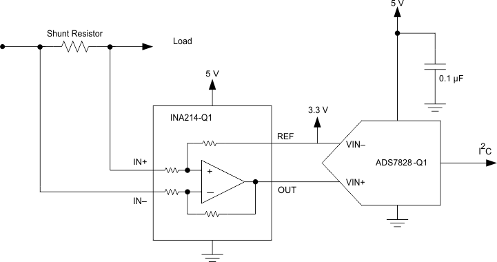 Figure 25. ADS7828-Q1 With Current Shunt Monitor
8.2.1.1 Design Requirements
For this design example, the ADS7828-Q1 device is paired with a current shunt monitor. Bi-directional current monitoring is required when there is both charging and discharging. The requirements for this example are as follows:
- Voltage across current shunt varies –15 mV to 15 mV
- 5-V supply
- 3.3-V rail available as reference
8.2.1.2 Detailed Design Procedure
8.2.1.2.1 Part Selection
The INA214-Q1 device was selected because of the low offset and zero drift of the device. The ADS7828-Q1 device has a low noise floor, so it can support more of the gain. For this reason, the lowest gain option was selected from the INA21x-Q1 family. The INA214-Q1 device has a gain of 50.
8.2.1.2.2 Full-Scale Differential Range
First, determine the full-scale differential range into the ADS7828-Q1 device.


8.2.1.2.3 Circuit Implementation
Because the ADS7828-Q1 device has a differential input, connect the reference voltage of the INA214-Q1 device to the negative input terminal of the ADS7828-Q1 device. Because bi-directional current sensing is required in this application, VREF must be chosen so that:


where
- Vfs = 3 V
A 3.3-V reference is used for this example. Because the ADS7828-Q1 device is a differential input ADC, a resistive divider can be used to generate the reference voltage because impedance effects on the INA214-Q1 device is canceled out by the ADS7828-Q1 device.
8.2.1.3 Application Curve
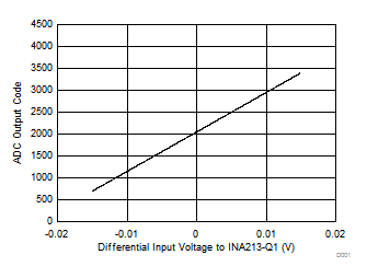 Figure 26. ADC Code vs Voltage Across Current-Shunt Resistor in Bi-Directional Current Sensing Application