ZHCSK88A September 2010 – September 2019 ADS7947 , ADS7948 , ADS7949
PRODUCTION DATA.
- 1 特性
- 2 应用
- 3 说明
- 4 修订历史记录
- 5 Device Comparison Table
- 6 Pin Configuration and Functions
-
7 Specifications
- 7.1 Absolute Maximum Ratings
- 7.2 ESD Ratings
- 7.3 Recommended Operating Conditions: ADS794x (12-, 10-, 8-Bit)
- 7.4 Thermal Information
- 7.5 Electrical Characteristics: ADS7947 (12-Bit)
- 7.6 Electrical Characteristics: ADS7948 (10-Bit)
- 7.7 Electrical Characteristics: ADS7949 (8-Bit)
- 7.8 Timing Requirements
- 7.9 Switching Characteristics
- 7.10 Typical Characteristics: ADS7947, ADS7948, ADS7949
- 7.11 Typical Characteristics: ADS7947 (12-Bit)
- 8 Detailed Description
- 9 Application and Implementation
- 10Power Supply Recommendations
- 11Layout
- 12器件和文档支持
- 13机械、封装和可订购信息
9.1 Application Information
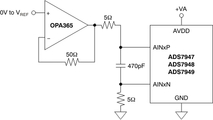
The device employs a sample-and-hold stage at the input; see Figure 40 for a typical equivalent circuit of a sample-and-hold stage. The device connects a 32-pF sampling capacitor during sampling. This configuration results in a glitch at the input terminals of the device at the start of the sample. The external circuit must be designed in such a way that the input can settle to the required accuracy during the sampling time chosen. Figure 53 shows a typical driving circuit for the analog inputs.
 Figure 53. Typical Input Driving Circuit
 The 470-pF capacitor across the AINxP and AINxN terminals decouples the driving op amp from the sampling glitch. Splitting the series resistance of the input filter in two equal values is recommended, as shown in Figure 53. Both input terminals are recommended to have the same impedance from the external circuit. The low-pass filter at the input limits noise bandwidth of the driving op amp. Select the filter bandwidth so that the full-scale step at the input can settle to the required accuracy during the sampling time. Equation 1, Equation 2, and Equation 3 are useful for filter component selection.

where


Also, make sure the driving op amp bandwidth does not limit the signal bandwidth below filter bandwidth. In many applications, signal bandwidth can be much lower than filter bandwidth. In this case, an additional low-pass filter can be used at the input of the driving op amp. This signal filter bandwidth can be selected in accordance with the input signal bandwidth.