ZHCSIJ3C June   2008  – July 2018 ADS7950 , ADS7951 , ADS7952 , ADS7953 , ADS7954 , ADS7955 , ADS7956 , ADS7957 , ADS7958 , ADS7959 , ADS7960 , ADS7961

PRODUCTION DATA.  

  1. 特性
  2. 应用
    1.     详细方框图
  3. 说明
  4. 修订历史记录
  5. 器件比较表
  6. Pin Configuration and Functions
    1.     Pin Functions: TSSOP Packages
    2.     Pin Functions: VQFN Packages
  7. Specifications
    1. 7.1  Absolute Maximum Ratings
    2. 7.2  ESD Ratings
    3. 7.3  Recommended Operating Conditions
    4. 7.4  Thermal Information: TSSOP
    5. 7.5  Thermal Information: VQFN
    6. 7.6  Electrical Characteristics: ADS7950, ADS7951, ADS7952, ADS7953
    7. 7.7  Electrical Characteristics, ADS7954, ADS7955, ADS7956, ADS7957
    8. 7.8  Electrical Characteristics, ADS7958, ADS7959, ADS7960, ADS7961
    9. 7.9  Timing Requirements
    10. 7.10 Typical Characteristics (All ADS79xx Family Devices)
    11. 7.11 Typical Characteristics (12-Bit Devices Only)
    12. 7.12 Typical Characteristics (12-Bit Devices Only)
  8. Detailed Description
    1. 8.1 Overview
    2. 8.2 Functional Block Diagram
    3. 8.3 Feature Description
      1. 8.3.1 Reference
      2. 8.3.2 Power Saving
    4. 8.4 Device Functional Modes
      1. 8.4.1 Channel Sequencing Modes
      2. 8.4.2 Device Programming and Mode Control
        1. 8.4.2.1 Mode Control Register
        2. 8.4.2.2 Program Registers
      3. 8.4.3 Device Power-Up Sequence
      4. 8.4.4 Operating in Manual Mode
      5. 8.4.5 Operating in Auto-1 Mode
      6. 8.4.6 Operating in Auto-2 Mode
      7. 8.4.7 Continued Operation in a Selected Mode
    5. 8.5 Programming
      1. 8.5.1 Digital Output
      2. 8.5.2 GPIO Registers
      3. 8.5.3 Alarm Thresholds for GPIO Pins
  9. Application and Implementation
    1. 9.1 Application Information
      1. 9.1.1 Analog Input
    2. 9.2 Typical Applications
      1. 9.2.1 Unbuffered Multiplexer Output (MXO)
        1. 9.2.1.1 Design Requirements
        2. 9.2.1.2 Detailed Design Procedure
        3. 9.2.1.3 Application Curves
      2. 9.2.2 OPA192 Buffered Multiplexer Output (MXO)
        1. 9.2.2.1 Design Requirements
        2. 9.2.2.2 Detailed Design Procedure
        3. 9.2.2.3 Application Curves
  10. 10Power Supply Recommendations
  11. 11Layout
    1. 11.1 Layout Guidelines
    2. 11.2 Layout Examples
  12. 12器件和文档支持
    1. 12.1 文档支持
      1. 12.1.1 相关文档
    2. 12.2 相关链接
    3. 12.3 接收文档更新通知
    4. 12.4 社区资源
    5. 12.5 商标
    6. 12.6 静电放电警告
    7. 12.7 术语表
  13. 13机械、封装和可订购信息

封装选项

请参考 PDF 数据表获取器件具体的封装图。

机械数据 (封装 | 引脚)
  • RGE|24
  • DBT|30
散热焊盘机械数据 (封装 | 引脚)
订购信息

Unbuffered Multiplexer Output (MXO)

This application is the most typical application, but requires the lowest RSOURCE for good performance. In this configuration, the 2xVREF range allows larger source impedance than the 1xVREF range because the 1xVREF range LSB size is smaller, thus making it more sensitive to settling error.
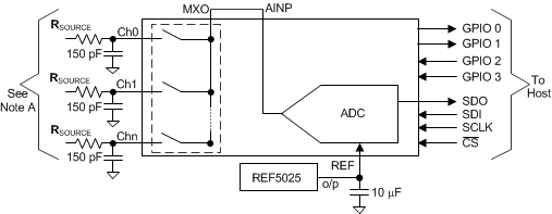
ADS7950 ADS7951 ADS7952 ADS7953 ADS7954 ADS7955 ADS7956 ADS7957 ADS7958 ADS7959 ADS7960 ADS7961 apps_nobuf.gif
A restriction on the source impedance exists. RSOURCE ≤ 100 Ω for the 1xVREF 12-bit settling at 1 MSPS or RSOURCE ≤ 250 Ω for the 2xVREF 12-bit settling at 1 MSPS.
Figure 63. Application Diagram for an Unbuffered MXO