ZHCSIJ3C June 2008 – July 2018 ADS7950 , ADS7951 , ADS7952 , ADS7953 , ADS7954 , ADS7955 , ADS7956 , ADS7957 , ADS7958 , ADS7959 , ADS7960 , ADS7961
PRODUCTION DATA.
- 1 特性
- 2 应用
- 3 说明
- 4 修订历史记录
- 5 器件比较表
- 6 Pin Configuration and Functions
-
7 Specifications
- 7.1 Absolute Maximum Ratings
- 7.2 ESD Ratings
- 7.3 Recommended Operating Conditions
- 7.4 Thermal Information: TSSOP
- 7.5 Thermal Information: VQFN
- 7.6 Electrical Characteristics: ADS7950, ADS7951, ADS7952, ADS7953
- 7.7 Electrical Characteristics, ADS7954, ADS7955, ADS7956, ADS7957
- 7.8 Electrical Characteristics, ADS7958, ADS7959, ADS7960, ADS7961
- 7.9 Timing Requirements
- 7.10 Typical Characteristics (All ADS79xx Family Devices)
- 7.11 Typical Characteristics (12-Bit Devices Only)
- 7.12 Typical Characteristics (12-Bit Devices Only)
- 8 Detailed Description
- 9 Application and Implementation
- 10Power Supply Recommendations
- 11Layout
- 12器件和文档支持
- 13机械、封装和可订购信息
封装选项
请参考 PDF 数据表获取器件具体的封装图。
机械数据 (封装 | 引脚)
- RHB|32
- DBT|38
散热焊盘机械数据 (封装 | 引脚)
- RHB|32
订购信息
8.4.6 Operating in Auto-2 Mode
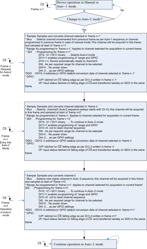
Figure 55 illustrates the steps involved in entering and operating in Auto-2 channel sequencing mode. Table 5 lists the mode control register settings for Auto-2 mode.
 Figure 55. Entering and Running in Auto-2 Channel Sequencing Mode
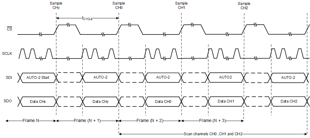
 Figure 56 shows an example in which Auto-2 mode is used to scan channels 0, 1, and 2. Auto-2 mode is selected to scan all channels until channel 2 (CH2) in ascending order by programming the Auto-2 register as described in Figure 56. The device enters Auto-2 mode on receiving the Auto-2 mode command in the Nth frame. This step causes the MUX to switch to CH0 in the (N+1)th frame. In the (N+2)th frame, the ADC samples and shifts out the conversion results for CH0 because the MUX internally switches to CH1. In the (N+3)th frame, the ADC samples and the shifts out the conversion result for CH1 and the MUX also switches to CH2, and so on. When this process reaches the maximum selected channel, CH2 in this case, the device returns to CH0 and repeats the cycle as long as the device remains in Auto-2 mode. Entering Auto-2 mode from any other mode also causes the device to restart from CH0. Additionally, modifying the contents of the for Auto-2 program register while operating in Auto-2 also causes the device to scan for restart from CH0.
 Figure 56. Example Auto-2 Mode Timing Diagram
 Table 5. Mode Control Register Settings for Auto-2 Mode
| BITS | RESET STATE | LOGIC STATE | FUNCTION | |||
|---|---|---|---|---|---|---|
| DI15-12 | 0001 | 0011 | Selects Auto-2 Mode | |||
| DI11 | 0 | 1 | Enables programming of bits DI10-00. | |||
| 0 | Device retains values of DI10-00 from the previous frame. | |||||
| DI10 | 0 | 1 | Channel number is reset to Ch-00. | |||
| 0 | Channel counter increments every conversion.(No reset). | |||||
| DI09-07 | 000 | xxx | Do not care | |||
| DI06 | 0 | 0 | Selects VREF i/p range (Range 1) | |||
| 1 | Selects 2xVREF i/p range (Range 2) | |||||
| DI05 | 0 | 0 | Device normal operation (no powerdown) | |||
| 1 | Device powers down on the 16th SCLK falling edge | |||||
| DI04 | 0 | 0 | SDO outputs the current channel address of the channel on DO15..12 followed by the 12-bit conversion result on DO11..00. | |||
| 1 | GPIO3-GPIO0 data (both input and output) is mapped onto DO15-DO12 in the order shown below. Lower data bits DO11-DO00 represent the 12-bit conversion result of the current channel. | |||||
| DO15 | DO14 | DO13 | DO12 | |||
| GPIO3(1) | GPIO2(1) | GPIO1(1) | GPIO0(1) | |||
| DI03-00 | 0000 | GPIO data for the channels configured as output. Device ignores data for the channel which is configured as input. SDI bit and corresponding GPIO information is given below | ||||
| DI03 | DI02 | DI01 | DI00 | |||
| GPIO3(1) | GPIO2(1) | GPIO1(1) | GPIO0(1) | |||
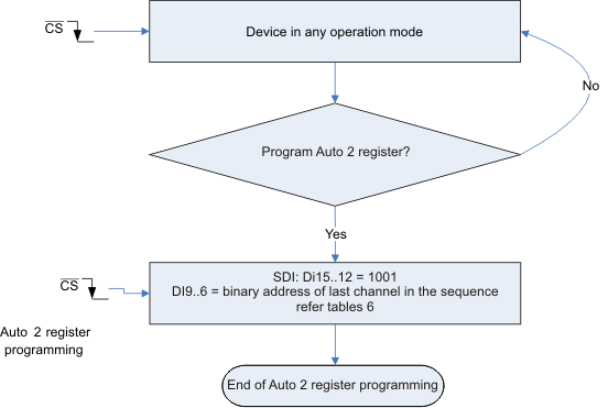
The Auto-2 Program Register is programmed (once on powerup or reset) to pre-select the last channel (or sequence depth) in the Auto-2 sequence. Unlike Auto-1 Program Register programming, Auto-2 Program Register programming requires only 1 CS frame for complete programming. See Figure 57 and Table 6 for complete details.

NOTE:
The device continues its operation in the selected mode during programming. SDO is valid, however it is not possible to change the range or write GPIO data into the device during programming.Table 6. Program Register Settings for Auto-2 Mode
| BITS | RESET STATE | LOGIC STATE | FUNCTION |
|---|---|---|---|
| DI15-12 | NA | 1001 | Auto-2 program register is selected for programming |
| DI11-10 | NA | Do not care | |
| DI09-06 | NA | aaaa | This 4-bit data represents the address of the last channel in the scanning sequence. During device operation in Auto-2 mode, the channel counter starts at CH-00 and increments every frame until it equals “aaaa”. The channel counter roles over to CH-00 in the next frame. |
| DI05-00 | NA | Do not care | |